Light emitting diode substrate, method of manufacturing the same, and liquid crystal display device using the same

a technology of light-emitting diodes and substrates, which is applied in the direction of lighting support devices, instruments, lighting applications, etc., can solve the problems of increasing manufacturing costs, reducing color uniformity, and complicating circuit configuration, so as to reduce manufacturing costs and improve color uniformity

Active Publication Date: 2007-08-23
SAMSUNG DISPLAY CO LTD
View PDF2 Cites 23 Cited by
  • Summary
  • Abstract
  • Description
  • Claims
  • Application Information

AI Technical Summary

Benefits of technology

[0008]The present invention provides an LED substrate that reduces manufacturing cost and improves color uniformity, a method of manufacturi

Problems solved by technology

However, color uniformity is less than what is desirable when using the primary color LEDs.
Th

Method used


Image

  • Light emitting diode substrate, method of manufacturing the same, and liquid crystal display device using the same
  • Light emitting diode substrate, method of manufacturing the same, and liquid crystal display device using the same
  • Light emitting diode substrate, method of manufacturing the same, and liquid crystal display device using the same

Examples


Embodiment Construction

[0017]The exemplary embodiments of the present invention will now be described with reference to FIGS. 1 to 4.

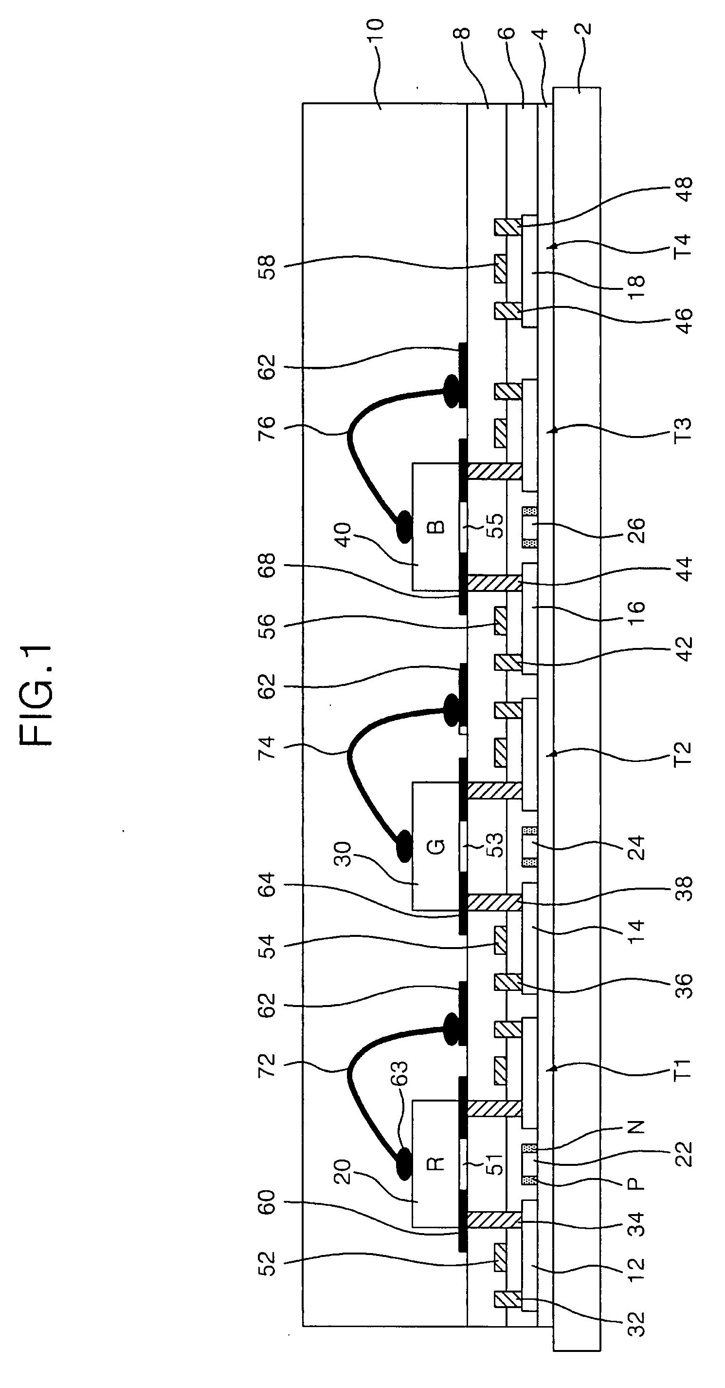
[0018]FIG. 1 is a cross-sectional view illustrating a part of an LED substrate according to an exemplary embodiment of the present invention.

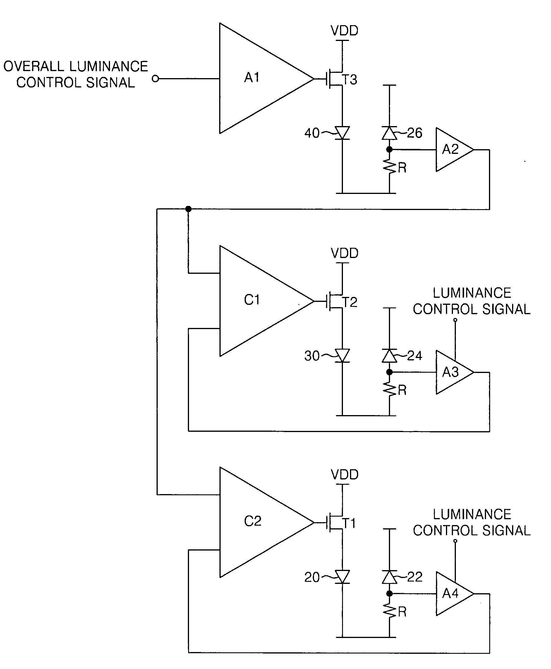
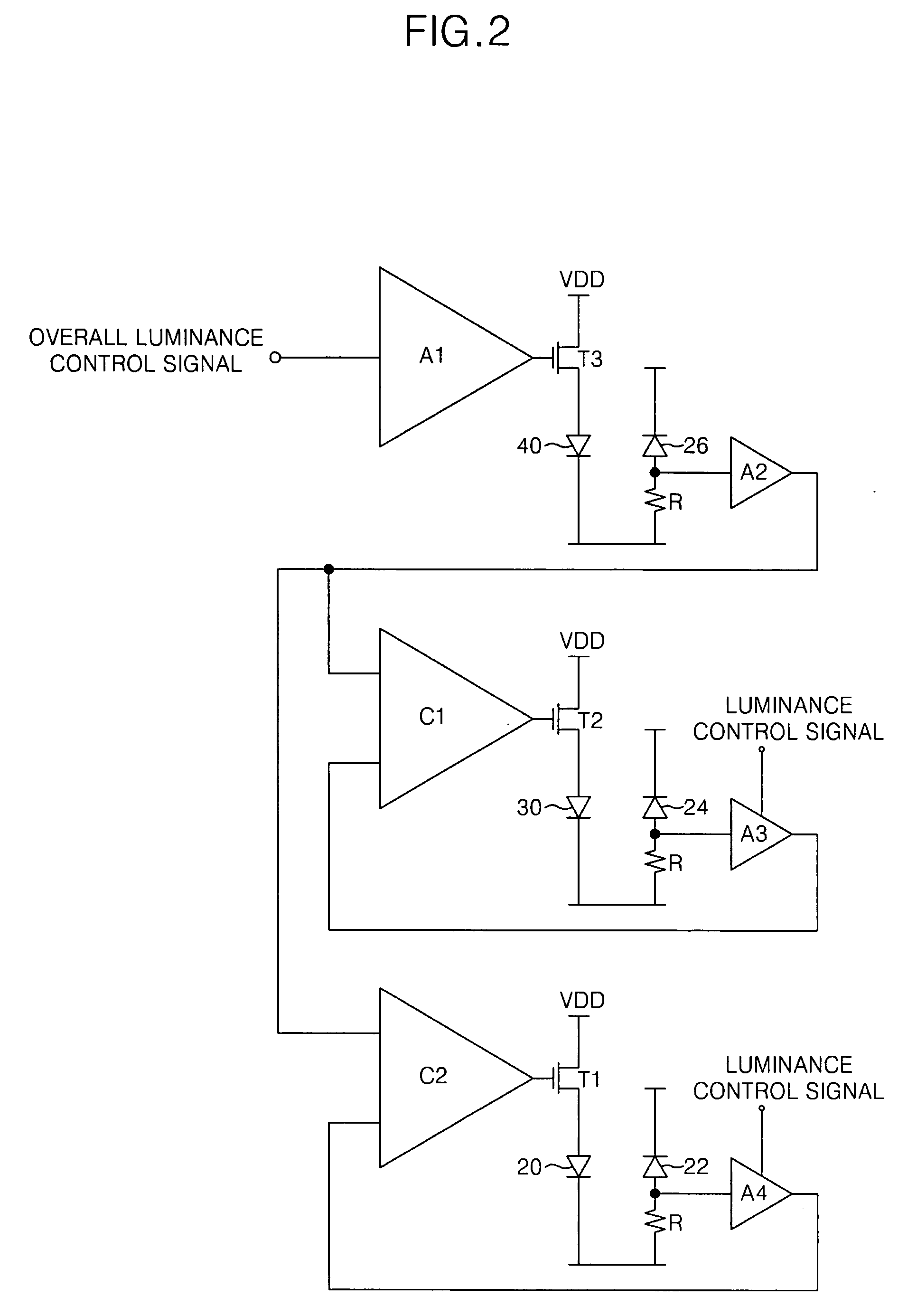
[0019]The LED substrate illustrated in FIG. 1 includes first to third thin film transistors (TFTs) T1, T2 and T3 for respectively driving R, G and B LEDs 20, 30 and 40, first to third thin film sensors 22, 24 and 26 for respectively detecting the luminous intensities of the R, G and B LEDs 20, 30 and 40, and a fourth TFT T4 contained in a luminance control circuit for controlling the first to third TFTs T1, T2 and T3. The first to fourth TFTs T1 to T4 and the first to third thin film sensors 22, 24 and 26 may use any one of polysilicon, polysilicon-germanium, amorphous silicon, and amorphous silicon-germanium thin films. However, for simplicity of explanation, the description will focus on the polysilicon thin film by way of example.

[00...


PUM


Abstract

A luminance control circuit for controlling the luminance levels of different colored light sources that lends itself to easy incorporation into display devices is presented. A light emitting diode (LED) substrate includes a plurality of driving thin film transistors (TFTs) including a semiconductor layer deposited on a substrate. A plurality of LEDs for generating lights of different wavelengths is mounted respectively on the plurality of driving TFTs. A plurality of thin film sensors for sensing the luminous intensities of the plurality of LEDs is formed between the plurality of LEDs and the substrate. A luminance control circuit for controlling the driving TFTs has of a plurality of controlling TFTs including a semiconductor layer deposited on the substrate and is connected to the plurality of thin film sensors.

Description

CROSS-REFERENCE TO RELATED APPLICATION(S)[0001]This application claims priority from Korean Patent Application No. 2006-0017527 filed in the Korean Patent Office on Feb. 23, 2006, the entire content of which is incorporated by reference herein.BACKGROUND OF THE INVENTION[0002]1. Field of the Invention[0003]The present invention relates to a light emitting diode device, and more particularly to a light emitting diode substrate with thin film light sensors integrated on the substrate.[0004]2. Description of the Related Art[0005]A liquid crystal display (LCD) device displays an image by using electro-optical properties of liquid crystals. Specifically, the LCD device includes an LCD panel for displaying an image through a pixel matrix and a driving circuit for driving the LCD panel. Since the LCD panel is a non-light-emitting device, the LCD device includes a backlight unit for supplying light to the LCD panel.[0006]The backlight unit typically uses a lamp as a light source but recentl...

Claims


Application Information

Patent Timeline
IPC IPC(8): G09G3/36H01L33/44
CPCG02F1/133603G02F1/133611G02F1/133615G09G3/3413G09G3/3611G09G2320/062H01L2224/73265G09G2320/0666G09G2360/147H01L2224/48091H01L2224/48464G09G2320/0633H01L2924/00014H01L2924/181H01L2924/00012A47F5/0043A47F13/00F21V21/02F21V23/04F21V33/0012F21W2131/301F21W2131/405
Inventor UEMOTO, TSUTOMU
Owner SAMSUNG DISPLAY CO LTD
Why Eureka
Try Eureka