Nonvolatile semiconductor memory device and data writing method

a semiconductor memory and data writing technology, applied in digital storage, electrical analogue stores, instruments, etc., can solve the problems of reducing voltage resistance, limiting the miniaturization of flash memory in a plane direction, and difficulty in arranging the contact hole at the same wiring interval as the word line and the bit lin

Inactive Publication Date: 2007-08-23
XENOGENIC DEV LLC
View PDF5 Cites 54 Cited by
  • Summary
  • Abstract
  • Description
  • Claims
  • Application Information

AI Technical Summary

Benefits of technology

[0052]According to the nonvolatile semiconductor memory device of the first or second characteristics, the variable resistive element that can store data by an electric resistance change by the application of the electric stress can be concretely implemented and the effect of the nonvolatile semiconductor memory device according to the first or second characteristics can be provided.

Problems solved by technology

Recently, problems in miniaturizing the flash memory includes a decrease in threshold voltage control due to lowering of a charge amount in a floating gate and a decrease in voltage resistance between a source and a drain due to reduction of a channel length, so that there is a limit of miniaturization of the flash memory in a plane direction.
Therefore, it is difficult to arrange the contact hole at the same wiring interval as that of the word line and the bit line arranged with the minimum processing line widths and intervals.
In addition, the variations in the programming time make it difficult to control the resistance value after the programming.
Furthermore, when the program current is set based on the memory cell that is slow in the programming time, the program current is excessive for the memory cell that is fast in the programming time, which could reduce the reliability of the memory cell.

Method used


Image

  • Nonvolatile semiconductor memory device and data writing method
  • Nonvolatile semiconductor memory device and data writing method
  • Nonvolatile semiconductor memory device and data writing method

Examples


first embodiment

[0080]First, a description will be made of a memory cell array in which data is written according to the method of the present invention. The memory cell array is constituted such that nonvolatile memory cells are arranged in rows and columns and information can be electrically written in the memory cell specified by an address inputted from the outside. Furthermore, information stored in the memory cell specified by an address input can be read out.

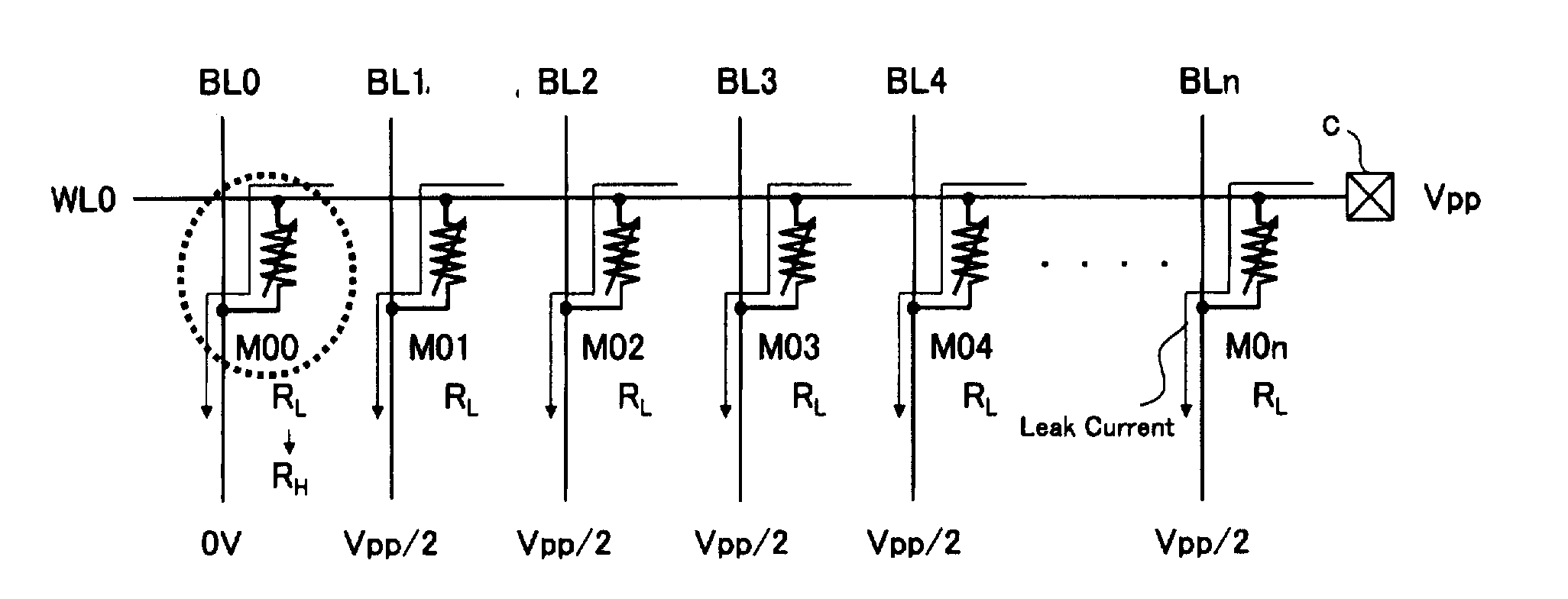
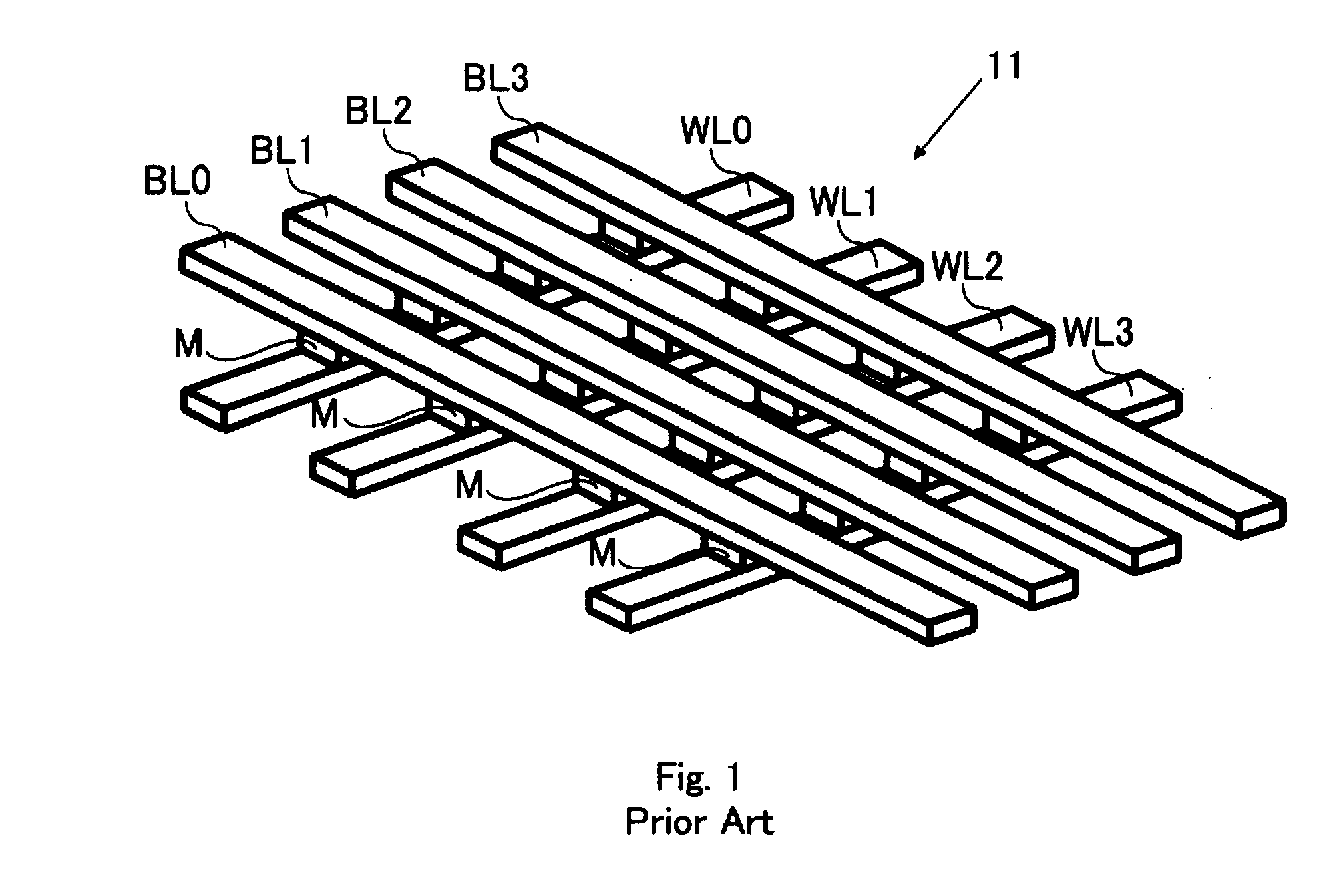
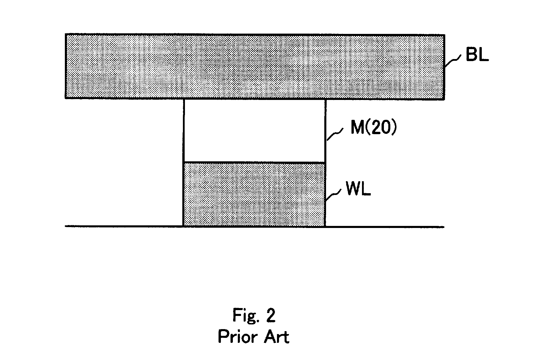
[0081]More specifically, the memory cell array has a cross-point type memory cell array structure in which two-terminal structured memory cells each having a variable resistive element storing information by the change of electric resistance are arranged in rows and columns, a plurality of word lines extending in a row direction and a plurality of bit lines extending in a column direction are provided, one ends of the memory cells in the same row is connected to the common word line, and the other ends of the memory cells in the same col...

example 1

[0111]A description will be made of a case where data is sequentially written along the word lines in the memory cell array in which the contact C of the word line is positioned in two ways: some are positioned at the right end while others are positioned at the left end according to the row address of the word line as shown in FIG. 6. Specifically, the contacts of the word line are positioned at the right ends in the even-numbered word lines WL0, WL2, WL4, . . . , and they are positioned at the left ends in the odd-numbered word lines WL1, WL3, WL5, . . . In addition, the reason why the contacts C are positioned as shown in FIG. 6 has been already described in the above “problems to be solved by the Invention”. A description will be made of the case where the programming is sequentially executed on the assumption that the memory cell array is controlled such that the resistance values of all memory cells are in the low resistance state (erase state) in the initial state before writ...

example 2

[0115]A description will be made of a case where data is sequentially written along word lines in a memory cell array in which contacts C are positioned at both right and left ends of the word line regardless of the row address of the word line as shown in FIG. 15. In addition, the arrangement of the contact C as shown in FIG. 15 can be implemented by devising the layout of a contact pad or enlarging the wiring distance between the word lines. A description will be made of a case where data is sequentially programmed in a memory cell array in which resistance values of all memory cells are controlled to be in the low resistance state (erase state) in the initial state before writing, hereinafter.

[0116]According to the method of the present invention, as shown in FIG. 16, the access order to each memory cell for programming is such that a word line WL0 designated by the lowest-order row address is selected first and then a bit line BL0 designated by the lowest-order column address is...


PUM


Abstract

The invention provides a data writing method for writing data sequentially in a cross-point memory cell array having a variable resistive element whose electric resistance is changed by application of an electric stress. When data is sequentially written in memory cells in the same row or column, the writing order of the memory cells to be written is determined according to the length from an electric connection point to a selected memory cell to be written and the increase/decrease direction of the electric resistance of each selected memory cell changed by data writing, the electric connection point being between a write voltage applying circuit, which applies a data writing voltage to a same wiring of the selected word line or bit line connected to the selected memory cell, and the same wiring, and the data writing is executed based on the determined writing order.

Description

CROSS REFERENCE TO RELATED APPLICATION[0001]This Nonprovisional application claims priority under 35 U.S.C. §119(a) on Patent Application No. 2006-046235 filed in Japan on 23 Feb., 2006, the entire contents of which are hereby incorporated by reference.BACKGROUND OF THE INVENTION[0002]1. Field of the Invention[0003]The present invention relates to a nonvolatile semiconductor memory device and more particularly, to a nonvolatile semiconductor memory device comprising a cross-point type memory cell array in which two-terminal structured memory cells each having a variable resistive element that can store data according to an electric resistance change by the application of an electric resistance are arranged in row and column directions, a plurality of word lines extending in a row direction and a plurality of bit lines extending in a column direction are provided, one ends of the memory cells in the same row are connected to the common word line, and the other ends of the memory cell...

Claims


Application Information

Patent Timeline
Patent Type & Authority Applications(United States)
IPC IPC(8): G11C11/00
CPCG11C13/0007G11C13/0069G11C2013/009G11C2213/77G11C2213/32G11C2213/34G11C2213/31
Inventor SUGITA, YASUHIRO
Owner XENOGENIC DEV LLC
Why Eureka
Try Eureka