Integrated vacuum metrology for cluster tool

a technology of integrated vacuum and clustering tool, which is applied in the direction of individual semiconductor device testing, semiconductor/solid-state device testing/measurement, instruments, etc., can solve the problem of varying device performance, affecting device performance, and the amount of allowable variability of device fabrication process uniformity and repeatability,

Inactive Publication Date: 2007-08-23
APPLIED MATERIALS INC
View PDF72 Cites 92 Cited by
  • Summary
  • Abstract
  • Description
  • Claims
  • Application Information

AI Technical Summary

Benefits of technology

[0012] In another embodiment, a method of processing a substrate is described. The method includes transferring a substrate to an evacuable chamber through an inlet valve coupled to the evacuable chamber, providing an environment in the evacuable chamber that is non-absorbing to wavelengths less than 200 nanometers, inspecting the substrate with an optical device that shares the environment in the evacuable chamber with the substrate, and transferring the substrate through an outlet valve after inspection.

Problems solved by technology

Due to the shrinking size of semiconductor devices and the ever increasing device performance requirements, the amount of allowable variability of the device fabrication process uniformity and repeatability, has greatly decreased.
If the substrate is exposed to atmospheric or other sources of contaminants for a time near or greater than the allowable queue time, the device performance may be affected by the contamination of the interface between the first and second layers.
Semiconductor device manufacturers spend a significant amount of time trying to reduce CoO issues created by substrate scrap due to misprocessed substrates, device defects or varying performance of the formed devices.
Typically, misprocessed substrates, device defects and / or varying device performance, may be caused by process drift in one or more of the processing chambers in a processing sequence, caused by contamination found in the system or process chambers, or caused by varying starting condition(s) of the substrate or layers of materials on the substrate.
Thus, production flow is effectively disrupted during transfer and inspection of the substrate or substrates.
Consequently, conventional metrology inspection methods can drastically increase overhead time associated with chip manufacturing.
Further, because such an inspection method is conducive only to periodic sampling due to the negative impact on throughput, many contaminated substrates can be processed without inspection, which may result in fabrication of defective devices.
Problems are compounded in cases where the substrates are redistributed from a given batch making it difficult to trace back to the contaminating source.

Method used


Image

  • Integrated vacuum metrology for cluster tool
  • Integrated vacuum metrology for cluster tool
  • Integrated vacuum metrology for cluster tool

Examples


Embodiment Construction

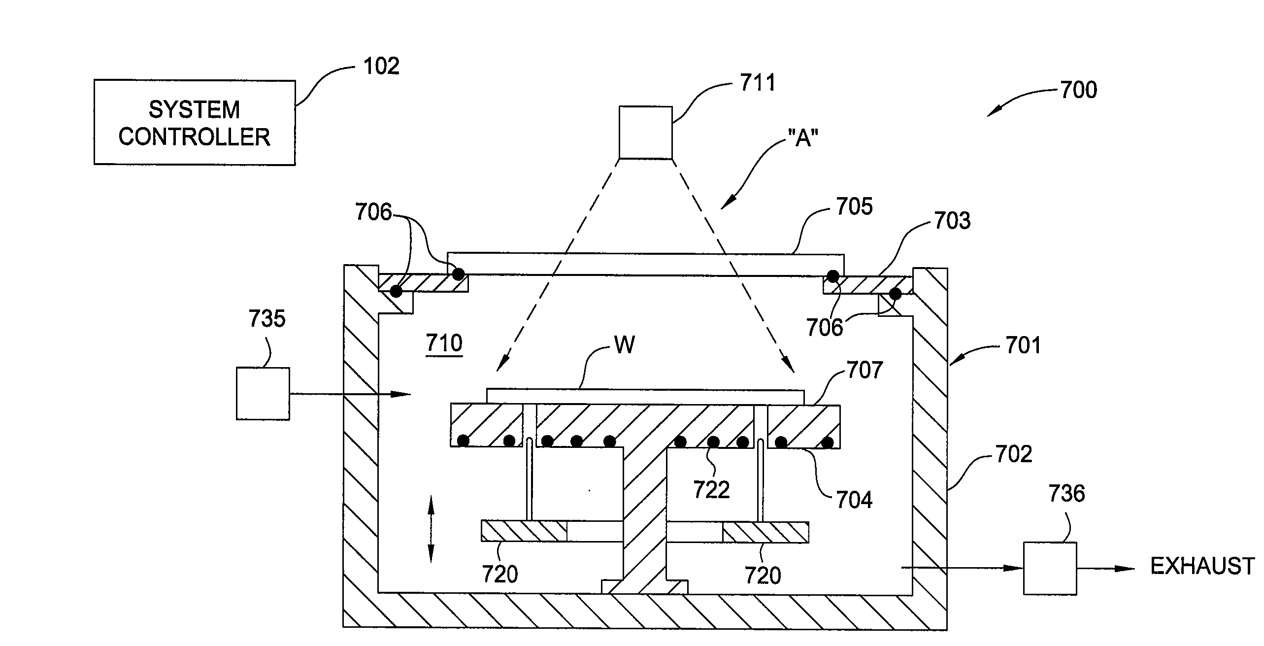
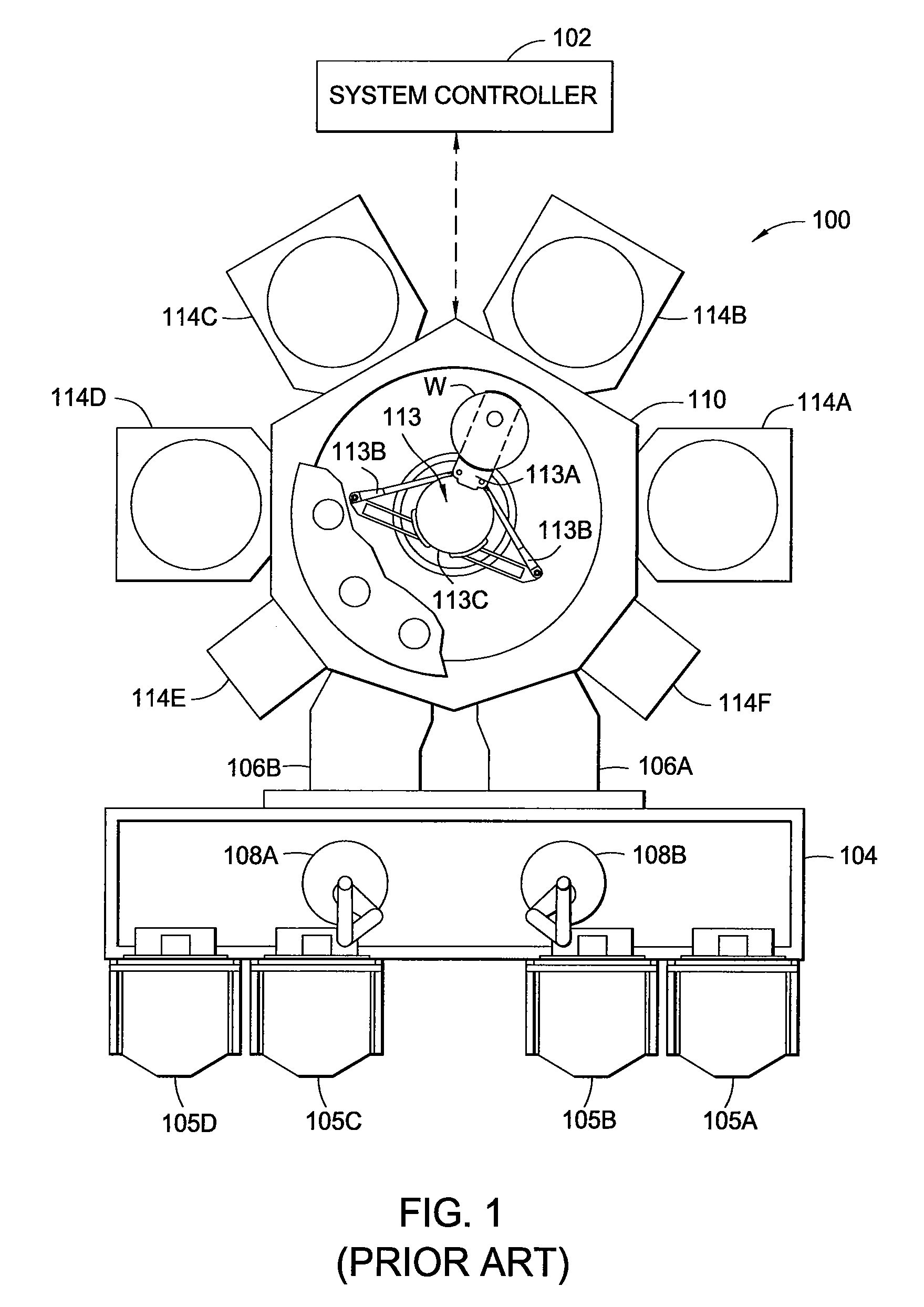
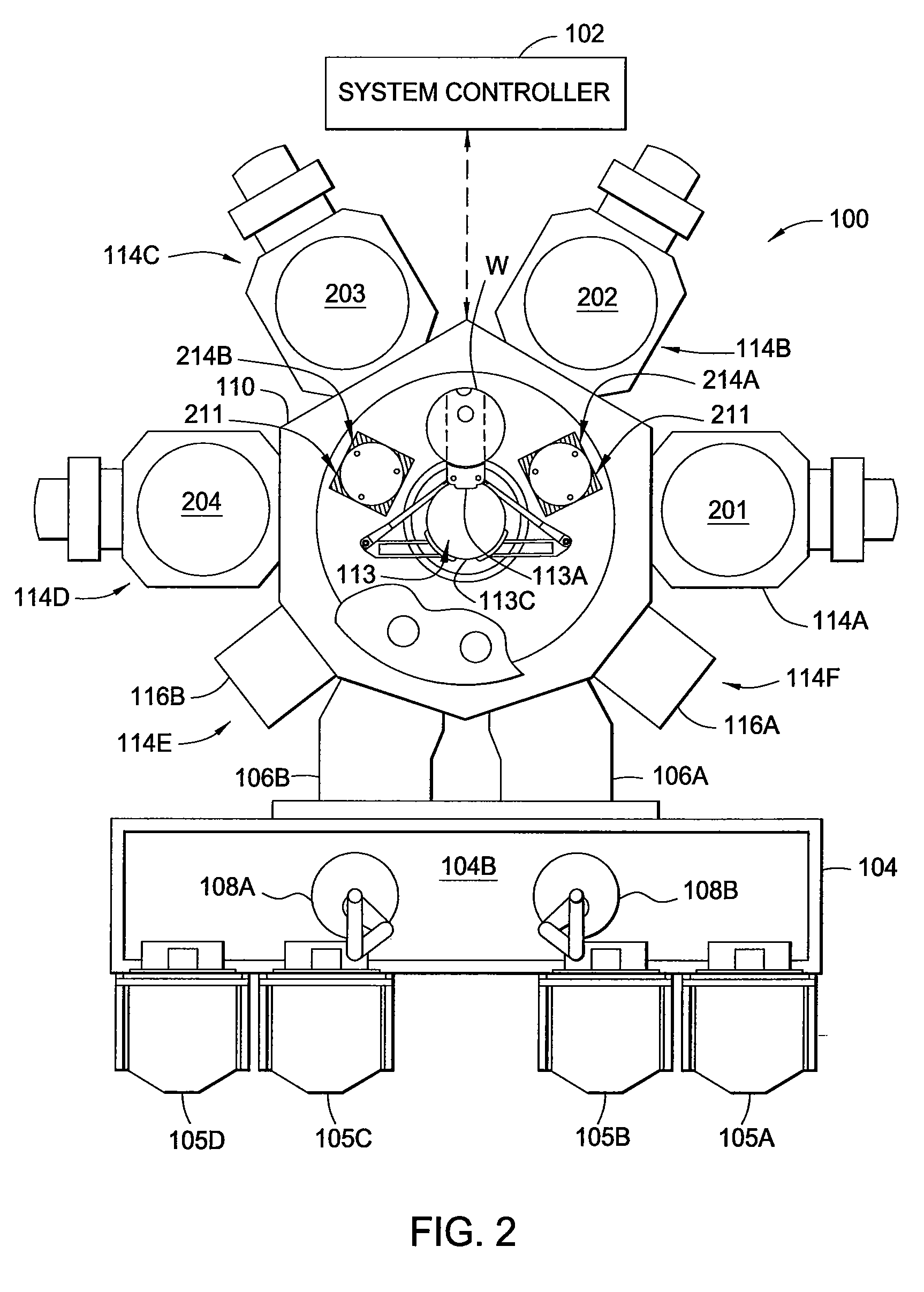
[0034] The present invention generally provides an apparatus and method for processing substrates using a multi-chamber processing system (e.g., a cluster tool) that is adapted to process substrates and analyze the results of the processes performed on the substrate. In one aspect of the invention, one or more analysis steps and / or precleaning steps are utilized to reduce the effect of queue time on device yield. In one aspect of the invention, a system controller and the one or more analysis chambers are utilized to monitor and control a process chamber recipe and / or a process sequence to reduce substrate scrap due to defects in the formed device and device performance variability issues. Embodiments of the present invention also generally provide methods and a system for repeatably and reliably forming semiconductor devices used in a variety of applications. The invention is illustratively described below in reference to a Centura® platform, available from Applied Materials, Inc.,...


PUM


Abstract

Aspects of the invention generally provide an apparatus and method for processing substrates using a multi-chamber processing system that is adapted to process substrates and analyze the results of the processes performed on the substrate. In one aspect of the invention, one or more analysis steps and/or pre-processing steps are performed on the substrate to provide data for processes performed on subsequent substrates. In one aspect of the invention, a system controller and one or more analysis devices are utilized to monitor and control a process chamber recipe and/or a process sequence to reduce substrate scrap due to defects in the formed device and device performance variability issues. Embodiments of the present invention also generally provide methods and a system for repeatably and reliably forming semiconductor devices used in a variety of applications.

Description

CROSS-REFERENCE TO RELATED APPLICATIONS [0001] This application is a continuation-in-part of U.S. patent application Ser. No. 11 / 460,864 (Attorney Docket No. 009526.P1), filed Jul. 28, 2006, which is a continuation-in-part of U.S. patent application Ser. No. 11 / 286,063 (Attorney Docket No. 009526), filed Nov. 22, 2005, which claims benefit of U.S. Provisional Patent Application Ser. No. 60 / 630,501 (Attorney Docket No. 009529L), filed Nov. 22, 2004, and U.S. Provisional Patent Application Ser. No. 60 / 642,877 (Attorney Docket No. 009526L02), filed Jan. 10, 2005, which are all herein incorporated by reference.BACKGROUND OF THE INVENTION [0002] 1. Field of the Invention [0003] Embodiments of the invention generally relate to an integrated processing system configured to perform processing steps on semiconductor substrates, and to perform testing and analysis of the substrates before and / or after processing. More particularly, the invention relates to integration of an analysis device in...

Claims


Application Information

Patent Timeline
Patent Type & Authority Applications(United States)
IPC IPC(8): H01L21/66G06K9/00
CPCG01N21/33H01L21/67109H01L21/67115H01L21/67745H01L21/67167H01L21/67196H01L21/67207H01L21/67161
Inventor COX, DAMON K.EGAN, TODDTHAKUR, RANDHIRSAMOILOV, ARKADIIHANSSON, PER-OVE
Owner APPLIED MATERIALS INC
Why Eureka
Try Eureka