Silicon substrate for magnetic recording medium, manufacturing method thereof, and magnetic recording medium

a technology of magnetic recording medium and silicon substrate, which is applied in the direction of magnetic materials for record carriers, manufacturing tools, instruments, etc., can solve the problems of fragile silicon substrates and defective products of magnetic recording media, and achieve the effect of preventing errors occurring during recording and reducing the rate of defective magnetic recording media

Inactive Publication Date: 2007-08-23
SHOWA DENKO KK
View PDF13 Cites 29 Cited by
  • Summary
  • Abstract
  • Description
  • Claims
  • Application Information

AI Technical Summary

Benefits of technology

[0018] According to the present invention, in a silicon substrate for a magnetic recording medium in which chamfer sections are provided between the main surface and the edge faces of the substrate, the edge faces and the chamfer sections of the substrate are of a mirror finish and a curved surface of greater than or equal to 0.01 mm and less than 0.3 mm radius is interposed between the main surface and the chamfer sections of the substrate. Therefore the corners of the substrate are smooth, the corners of the substrate do not chip off, there is no occurrence of particles from the substrate, and debris from rubbing against the process cassette can be prevented. Hence it is possible to reduce the rate of defective magnetic recording media occurring, and prevent errors occurring during recording and reproduction.

Problems solved by technology

However, since silicon substrates are fragile, with substrates of the shape disclosed in Japanese Patent Application, First Publication No.
Therefore, chips occur on the substrate edge faces and cracks occur on the substrates due to shocks during transport, and particle contamination occurs from debris of silicon powder produced by rubbing against the process cassette, causing defective magnetic recording media products to occur.

Method used


Image

  • Silicon substrate for magnetic recording medium, manufacturing method thereof, and magnetic recording medium
  • Silicon substrate for magnetic recording medium, manufacturing method thereof, and magnetic recording medium
  • Silicon substrate for magnetic recording medium, manufacturing method thereof, and magnetic recording medium

Examples


embodiment

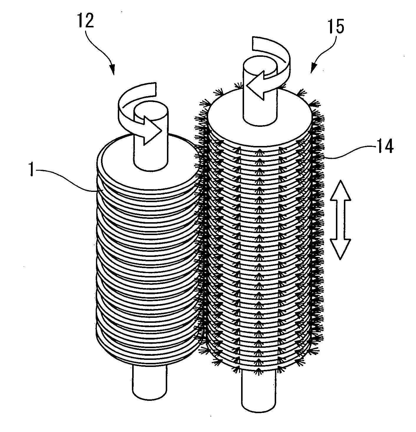
[0068] A silicon substrate with a diameter of 150 mm (nominal: 6 inches) was prepared, a first stage lapping process, a laser cutting process, a second lapping process, an inner and outer peripheral chamfer process, an inner and outer peripheral edge brushing process, a main surface first polishing process, and a main surface second polishing process, were performed in sequence, and twenty 0.85 inch silicon substrates with a shape as shown in Table 2 were produced.

[0069] A stack of silicon substrates, in which spacers made from epoxy resin with a diameter of 21 mm and a thickness of 0.2 mm were inserted between the silicon substrates, was used in the polishing process and the brushing process of the inner and outer peripheral edge faces.

[0070] In the brushing process of the inner peripheral edge faces, a polishing brush formed from a bundle of polyamide fibers with a diameter of 0.1 mm and a length of 5 mm, formed in a spiral, was used, and a polishing liquid was used in which alu...


PUM

PropertyMeasurementUnit
radiusaaaaaaaaaa
radiusaaaaaaaaaa
lengthaaaaaaaaaa

Abstract

A silicon substrate for magnetic recording medium is provided, which, even though it is a silicon substrate of a fragile material, is not prone to chip on the substrate edge faces or cracks on the substrate, and which prevents debris from being produced from the substrate edge faces, and which prevents debris from being produced by rubbing against a process cassette. Therefore, in a silicon substrate for a magnetic recording medium, in which there is provided a chamfer section between a main surface of the substrate and an edge face, the edge face and chamfer section of the substrate are of mirror finish, and a curved surface with a radius of greater than or equal to 0.01 mm and less than 0.3 mm is interposed between the main surface of the substrate and the chamfer section. In forming the curved surface, a silicon substrate stack with a plurality of silicon substrates and spacers laminated is prepared, and the inner periphery of a central hole of the substrates, and an outer periphery of the substrates are brush polished.

Description

TECHNICAL FIELD [0001] The present invention relates to a silicon substrate for a small size magnetic recording medium, which is used as a recording medium for information-processing equipment. [0002] Priority is claimed on Japanese Patent Application No. 2004-234366, filed Aug. 11, 2004, Japanese Patent Application No.2005-122175, filed Apr. 20, 2005, and U.S. Provisional application No. 60 / 603,272, filed Aug. 23, 2004, the content of which are incorporated herein by reference. BACKGROUND ART [0003] As the range of information equipment has expanded in recent years, the memory capacity of magnetic recording media has continued to increase. Especially, magnetic discs which play a major role as the external memory of computers, increase their memory capacity and memory density year by year. However, development is required in order to perform higher density recording. For example, due to the development of notebook type personal computers and palm top personal computers, a small size...

Claims


Application Information

Patent Timeline
Patent Type & Authority Applications(United States)
IPC IPC(8): G11B5/706B24B7/30B24B1/00
CPCB24B1/00G11B5/8404G11B5/7315B24B9/065G11B5/73911
Inventor AIDA, KATSUAKI
Owner SHOWA DENKO KK
Why Eureka
Try Eureka