III-V group compound semiconductor light-emitting diode

a light-emitting diode, compound semiconductor technology, applied in the direction of semiconductor devices, basic electric elements, electrical appliances, etc., can solve the problem that the largest factor limiting the light-emitting efficiency of a light-emitting diode cannot be allowed to escape it is difficult to efficiently extract the light generated in the active layer to the outside space, etc., to achieve high efficiency, efficiently suppress the total internal reflection, and high efficiency

Inactive Publication Date: 2007-08-30
NAT INST OF ADVANCED IND SCI & TECH
View PDF10 Cites 50 Cited by
  • Summary
  • Abstract
  • Description
  • Claims
  • Application Information

AI Technical Summary

Benefits of technology

[0007] The present invention contemplates providing a highly efficient light-emitting diode using a III-V group compound semiconductor as a raw material, the light-emitting diode being perfectly free, in principle, from the above problem concerning light blocking caused by a metal electrode, and being able to efficiently suppress the total internal reflection at the interface. Further, the present invention also contemplates providing a highly efficient light-emitting diode using a III-V group compound semiconductor as a raw material, the light-emitting diode allowing high output light power to be easily obtained from a single chip, as the output light power of a light-emitting diode increases in proportion to area of the chip.

Problems solved by technology

On the other hand, it is very difficult to efficiently extract the light generated in the active layer to the outside space.
It is not too much to say that this is the largest factor limiting the light-emitting efficiency of a light-emitting diode.
Therefore, the light is not allowed to escape to the outside space.
However, even if any of these structures is adopted, the situation where the density of current just under the metal electrode or in the vicinity thereof is the highest of all is not changed, and the effects of these structures are limited.
Further, these structures give rise to the problem that the introduction of the thick current-spreading layer or current-blocking layer complicates production processes of such the devices and raises production cost.
Thus, there is a limitation to the output power of light obtained from one light-emitting diode chip.

Method used


Image

  • III-V group compound semiconductor light-emitting diode
  • III-V group compound semiconductor light-emitting diode
  • III-V group compound semiconductor light-emitting diode

Examples


Embodiment Construction

[0036] Some embodiments according to the present invention will be explained in below, with reference to FIGS. 1 to 10, but the invention is not intended to be limited thereto.

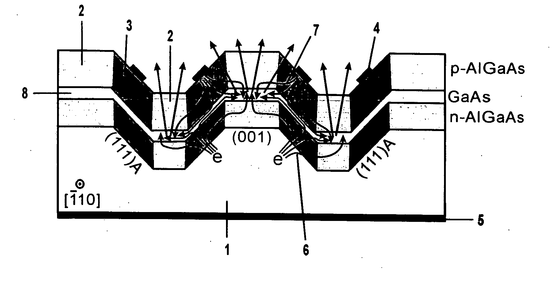
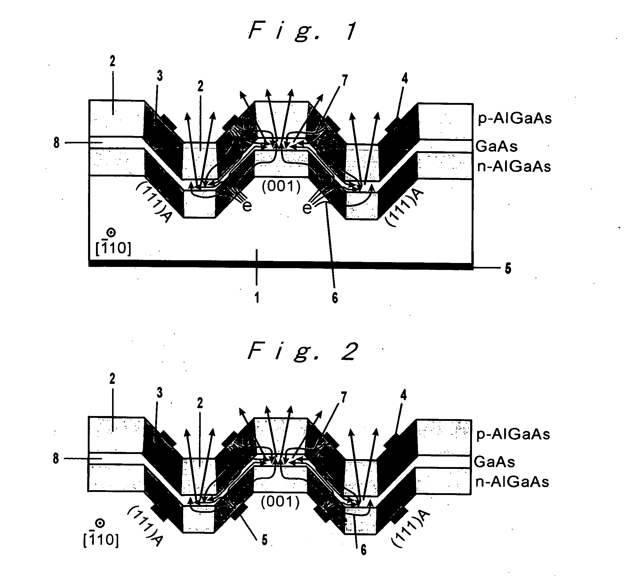
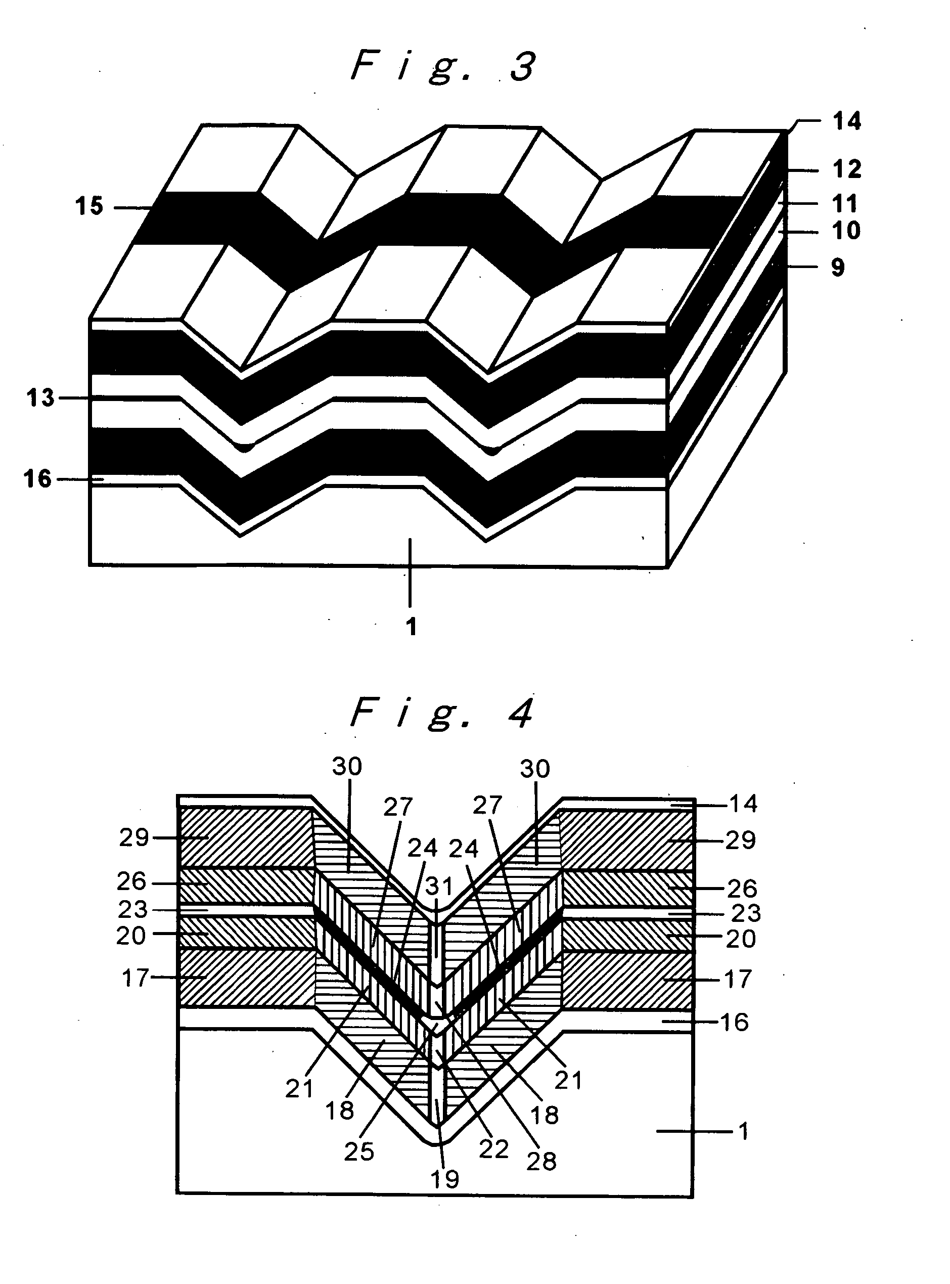
[0037]FIGS. 1 and 2 each are a schematic sectional view for explaining fundamental structure of the III-V group compound semiconductor light-emitting diode according to an embodiment of the present invention.

[0038] In these figures, reference numeral 1 represents a n-type (001) GaAs substrate, 2 represents an AlGaAs region with a lower Al composition of an AlGaAs barrier layer, 3 represents an AlGaAs region with a higher Al composition of an AlGaAs barrier layer, 4 represents a p-type Ohmic electrode, 5 represents a n-type Ohmic electrode, 6 represents the migration direction of electrons, 7 represents the migration direction of holes, and 8 represents a GaAs quantum well active layer.

[0039] The fundamental structure of the III-V group compound semiconductor light-emitting diode of the present invention wil...


PUM


Abstract

A III-V group compound semiconductor light-emitting diode, containing a substrate 1 having plural crystal planes, and a grown layer formed on the substrate by epitaxial growth, the grown layer at least including a barrier layer 2 and 3 and an active layer 8, wherein at least the active layer of the grown layer has plural crystal planes each having a different bandgap energy in the in-plane direction, and an Ohmic electrode 4 for current injection is formed on a crystal plane (3) having a higher bandgap energy among the plural crystal planes.

Description

FIELD OF THE INVENTION [0001] The present invention relates to a high-efficiency light-emitting diode using a III-V group compound semiconductor as a raw material, and, specifically to a III-V group compound semiconductor light-emitting diode which is improved in the efficiency of extracting light to the outside space, by separating a light-extraction area from a current-injection area. BACKGROUND OF THE INVENTION [0002] There is great current interest in a light-emitting diode, whose raw material is a III-V group compound semiconductor (for example, AlGaAs, AlGaInP and AlGaInN), as an energy saving and long-lifetime light source for lighting devices in the next generation which will be used in place of an incandescent lamp and a fluorescent lamp. [0003] The light-emitting efficiency of a light-emitting diode is generally determined by the product of the internal quantum efficiency and the efficiency of extraction of light to the outside space. With regard to internal quantum effici...

Claims


Application Information

Patent Timeline
Patent Type & Authority Applications(United States)
IPC IPC(8): H01L33/00H01L33/16H01L33/24H01L33/30
CPCH01L33/0079H01L33/30H01L33/24H01L33/16H01L33/0093
Inventor WANG, XUE-LUN
Owner NAT INST OF ADVANCED IND SCI & TECH
Why Eureka
Try Eureka