Method for producing partial soi structures comprising zones connecting a superficial layer and a substrate

a technology of surface layer and substrate, applied in the direction of microstructured devices, microstructured technology, microstructured devices, etc., can solve problems such as heterogeneous surface conditions

Active Publication Date: 2007-08-30
S O I TEC SILICON ON INSULATOR THECHNOLOGIES
View PDF8 Cites 34 Cited by
  • Summary
  • Abstract
  • Description
  • Claims
  • Application Information

AI Technical Summary

Problems solved by technology

In this type of method, one problem is that of having to condition a heterogeneous surface.

Method used


Image

  • Method for producing partial soi structures comprising zones connecting a superficial layer and a substrate
  • Method for producing partial soi structures comprising zones connecting a superficial layer and a substrate
  • Method for producing partial soi structures comprising zones connecting a superficial layer and a substrate

Examples


example 1

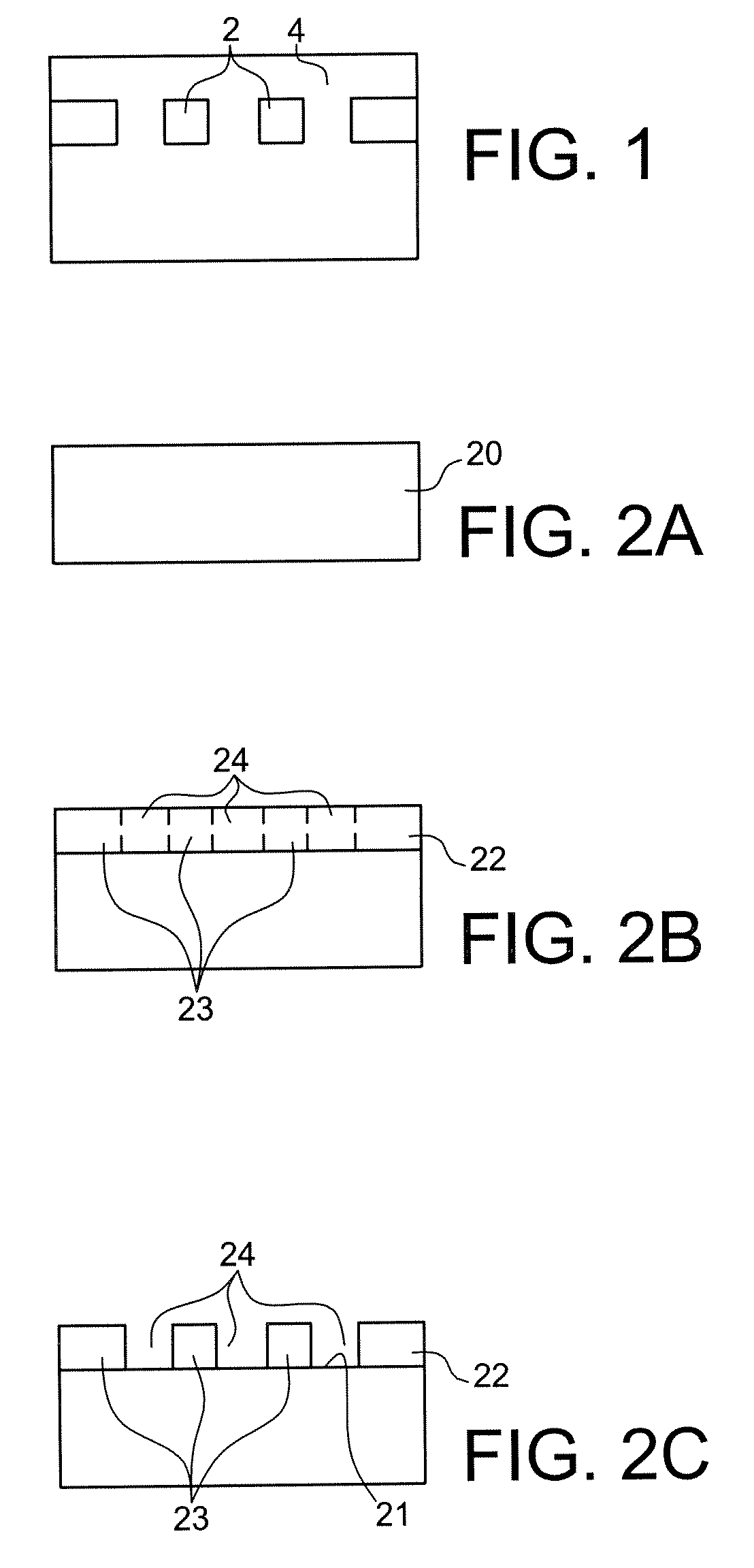
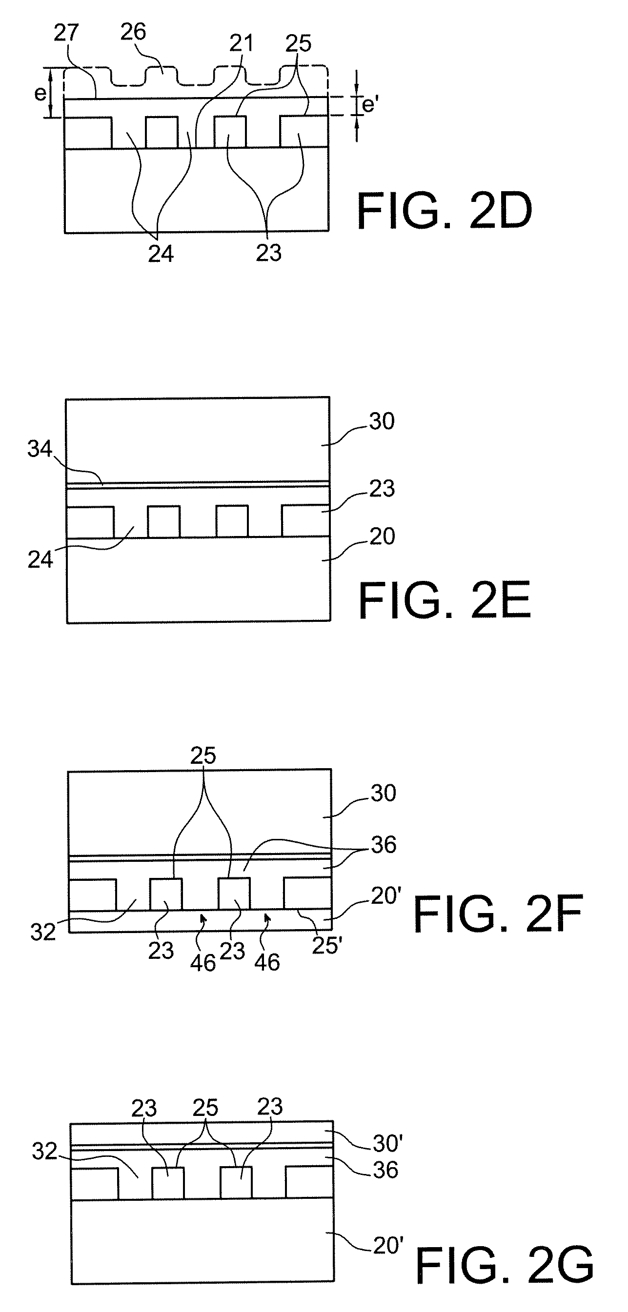
[0078]In this example, the following steps are performed:[0079]a1) thermal oxidation of a silicon substrate 20, for example by generating 2 μm of oxide;[0080]b1) lithography of the patterns 24 to define future SOI and Si zones;[0081]c1) etching of the oxide 22 at the level of the future Si zones defined and removal of the etching mask;[0082]d1) cleaning of the surface and deposition of a polycrystalline silicon (p-Si) layer 26 by LPCVD (at around 650° C.), for example, deposition of a layer having a thickness of around 4 μm;[0083]e1) heat treatment at 1100° C.;[0084]f1) planarisation of the p-Si surface 26 so as to remove the topology between the SOI and Si zones by chemical-mechanical polishing; however, one remains on a homogenous poly-Si surface, and never move onto a heterogeneous SiO2 / Si surface;[0085]g1) hydrophilic-type cleaning and placement in contact for direct bonding by molecular adhesion of the substrate 20—pattern 23—layer 26 assembly and a silicon-free substrate 30;[0...

example 2

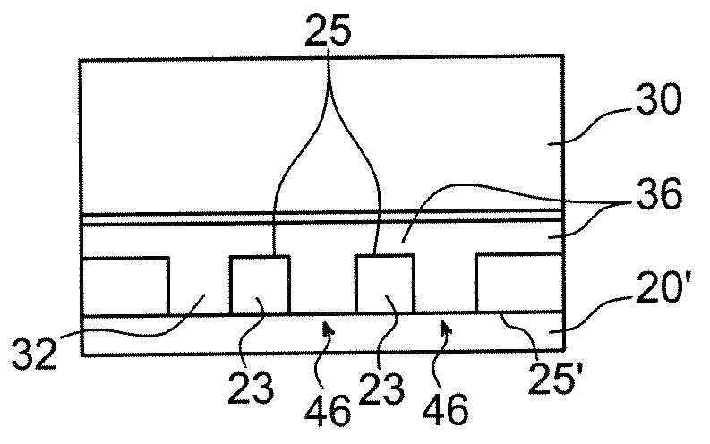
[0088]In this example, the following steps are performed:[0089]steps a2 to c2: same as steps a1 to c1.[0090]d2) cleaning of the surface and deposition of an amorphous silicon (a-Si) layer 26 by PECVD, for example, deposition of a layer having a thickness of around 5 μm;[0091]e2) heat treatment at 1100° C.;[0092]f2) planarisation of the a-Si surface 26 so as to remove the topology between the SOI and Si zones by chemical-mechanical polishing;[0093]g2) hydrophobic-type cleaning and placement in contact for direct bonding by molecular adhesion of the substrate 20 and a silicon-free substrate 30;[0094]h2) same as h1;[0095]i2) thinning of the rear surface of the substrate 30 by mechanical grinding, then by chemical-mechanical polishing, for example until a thickness of 20 μm is obtained. A structure as shown in FIG. 2G is thus obtained.

example 3

[0096]In this example, the following steps are performed:[0097]a3) thermal oxidation of a silicon substrate 20, for example by generating 3 μm of oxide;[0098]b3) to c3) : same as b1) to c1);[0099]d3) cleaning of the surface and deposition of a polycrystalline silicon (p-Si) layer 26 by LPCVD (at around 650° C.), for example, deposition of a layer having a thickness of around 7 μm;[0100]e3) same as e1);[0101]f3) planarisation of the p-Si surface 26 so as to remove the topology between the SOI and Si zones by dry polishing, then surface finishing by chemical-mechanical polishing;[0102]g3) to h3) : same as g1) to h1);[0103]i3) thinning of the rear surface of the substrate 20 by mechanical grinding, then by chemical-mechanical polishing, for example until a thickness of 20 μm is obtained. A structure as shown in FIG. 2F is thus obtained.


PUM


Abstract

The invention relates to a method for producing a semiconductor structure comprising a superficial layer, at least one embedded layer, and a support, which method comprises:
  • a step of forming, on a first support, patterns in a first material,
  • a step of forming a semiconductor layer, between and on said patterns,
  • a step of assembling said semiconductor layer with a second support.

Description

TECHNICAL FIELD AND PRIOR ART[0001]The invention relates to the production of new structures of semiconductor components or MEMS-type devices, and in particular SOI or SOI-type devices.[0002]Numerous microsystems or MEMS (Micro Electro Mechanical Systems) are produced using SOI (Silicon On Insulator) materials, which make it possible in particular to obtain monocrystalline silicon membranes suspended above a cavity.[0003]In various applications in the field of power electronics and microsystems, it can be advantageous to have a structure combining the functions of a “bulk” silicon substrate and an SOI substrate: i.e. comprising local zones 2 of embedded oxide (for example SiO2) under an active layer 4, as shown in FIG. 1.[0004]To obtain this type of structure, a number of methods have already been described, for example in document FR 0216646.[0005]In this type of method, one problem is that of having to condition a heterogeneous surface.[0006]The problem of producing a structure co...

Claims


Application Information

Patent Timeline
Patent Type & Authority Applications(United States)
IPC IPC(8): H01L29/739
CPCB81C1/00357B81C1/0038B81C2201/019H01L21/76251H01L21/76254Y10T428/12674H01L21/02532H01L21/0254H01L21/0262H01L21/02639H01L21/02381H01L27/12H01L21/20
Inventor ASPAR, BERNARDLAGAHE-BLANCHARD, CHRYSTELLE
Owner S O I TEC SILICON ON INSULATOR THECHNOLOGIES
Why Eureka
Try Eureka