Method of Evaluating Quality of Silicon Single Crystal

a technology of silicon single crystal and quality inspection, applied in the direction of polycrystalline material growth, crystal growth process, polycrystalline material growth, etc., can solve the problems of reducing yield, reducing quality standards, and increasing demands on silicon wafer quality, so as to avoid discarding satisfactory wafers, improve operational efficiency, and improve quality inspection accuracy

Inactive Publication Date: 2008-12-11
SUMCO TECHXIV
View PDF1 Cites 8 Cited by
  • Summary
  • Abstract
  • Description
  • Claims
  • Application Information

AI Technical Summary

Benefits of technology

[0022]According to the present invention, log data of the control parameters during crystal growth is employed to evaluate the quality of all parts of the silicon single crystal. Because all parts of the silicon single crystal are evaluated, the accuracy of the quality inspection can be said to be comparatively higher than the conventional sampling inspection in which only a part of the silicon single crystal is extracted and evaluated. In addition, the satisfactory product part and unsatisfactory product part can be reliably distinguished. Accordingly, the implementation of wafer finishing processing on unsatisfactory wafers is avoided and the operational efficiency is improved. In addition, the discarding of satisfactory wafers is avoided and yield is improved.

Problems solved by technology

A demand for higher integration degree and miniaturization of semiconductor devices have arisen in recent years, and this demand has been accompanied by increasingly severe demands in terms of silicon wafer quality.
Grown-in defects have an undesirable effect during semiconductor device processing on, for example, the dielectric strength and leakage current characteristics of the insulating oxide film, and are a cause of reduced yield.
At the hitherto employed control levels, however, a partial failure to meet the quality standards occurs and the need for a more accurate inspection and judgment thereof arises.
On the other hand, although it is possible to detect the ID by a non-destructive evaluation method, such a method has a problem for the practical application in the regular inspection because of the extremely low ID density of the order of 103 to 104 / cm3.

Method used


Image

  • Method of Evaluating Quality of Silicon Single Crystal
  • Method of Evaluating Quality of Silicon Single Crystal
  • Method of Evaluating Quality of Silicon Single Crystal

Examples


Embodiment Construction

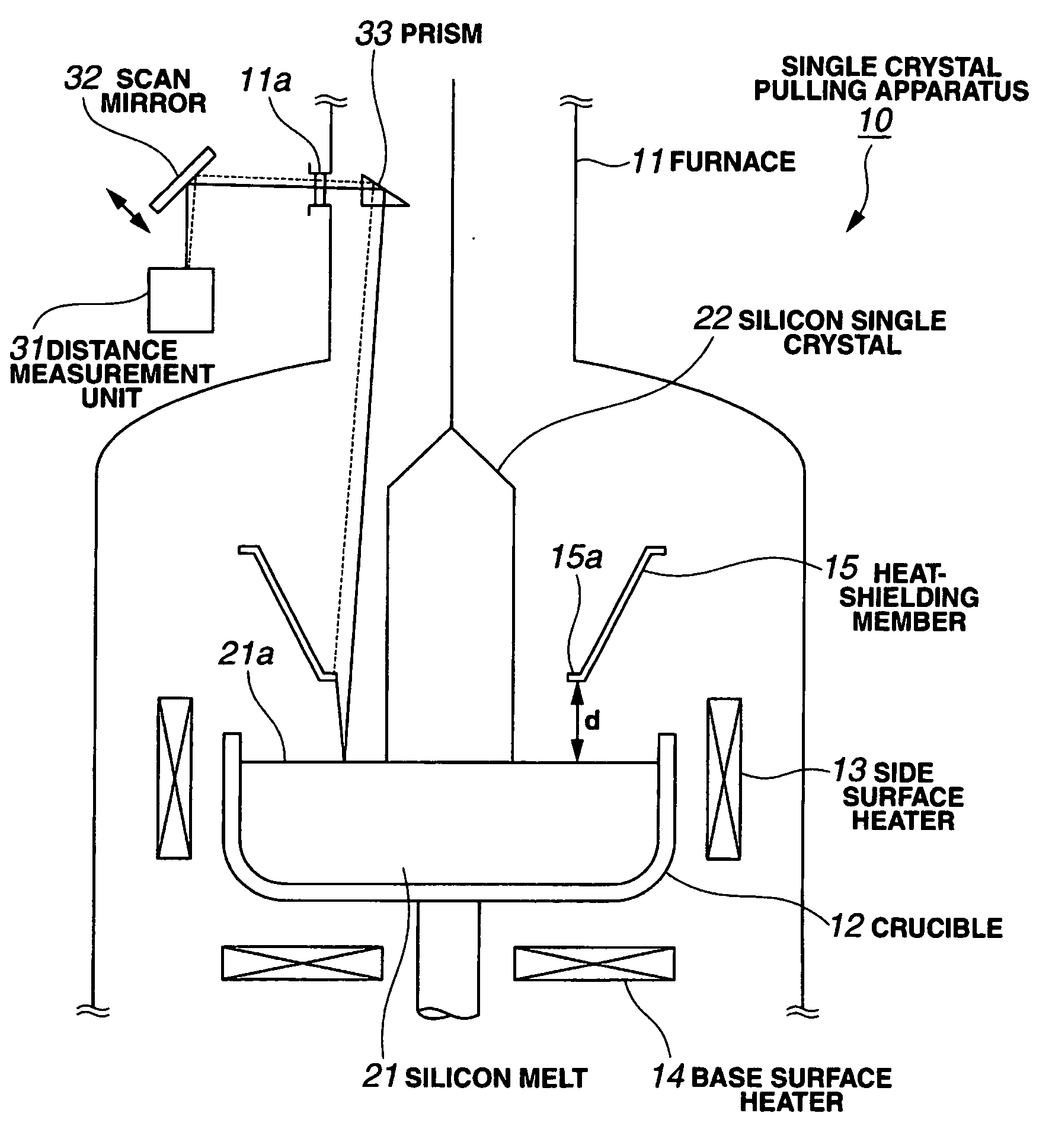
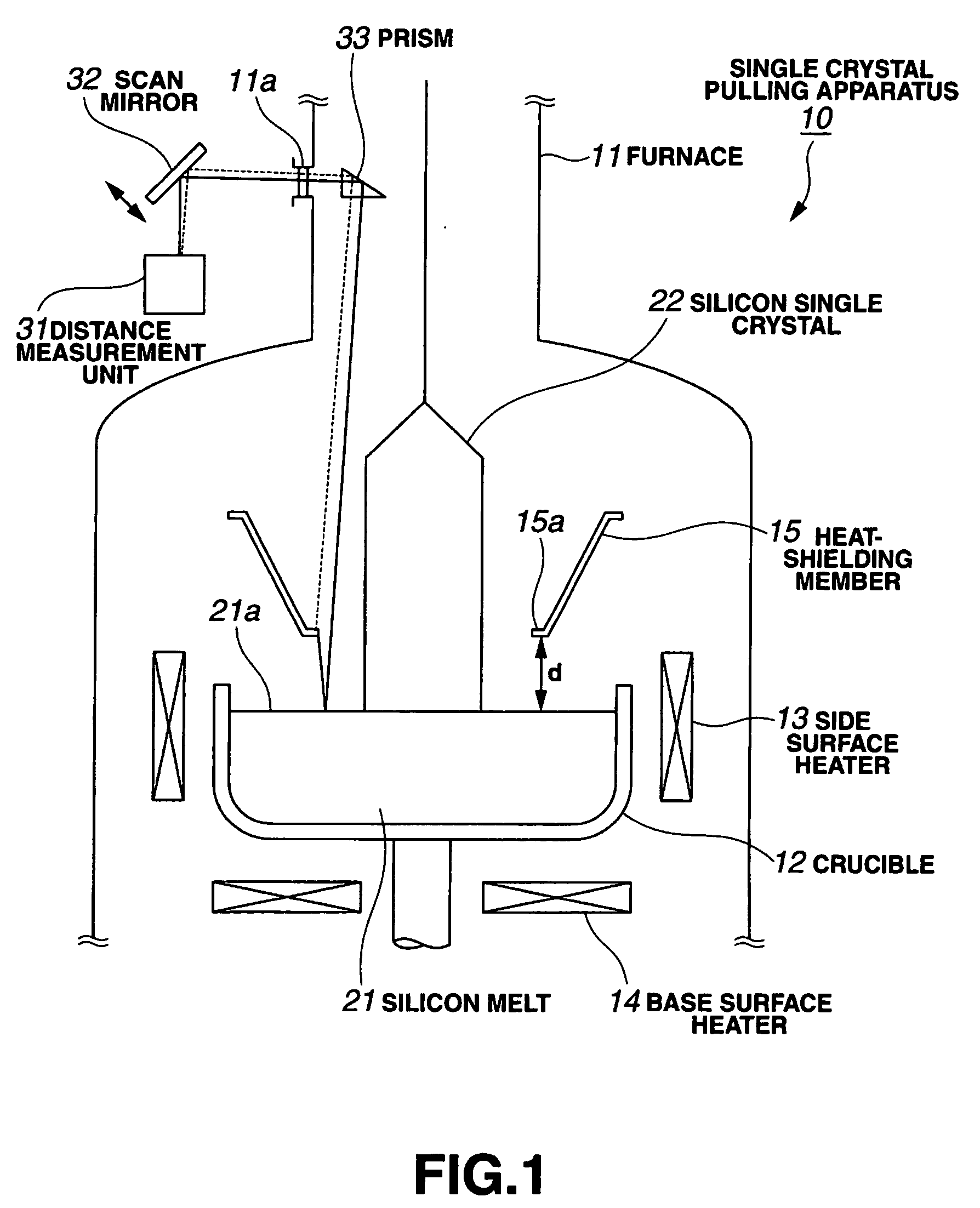
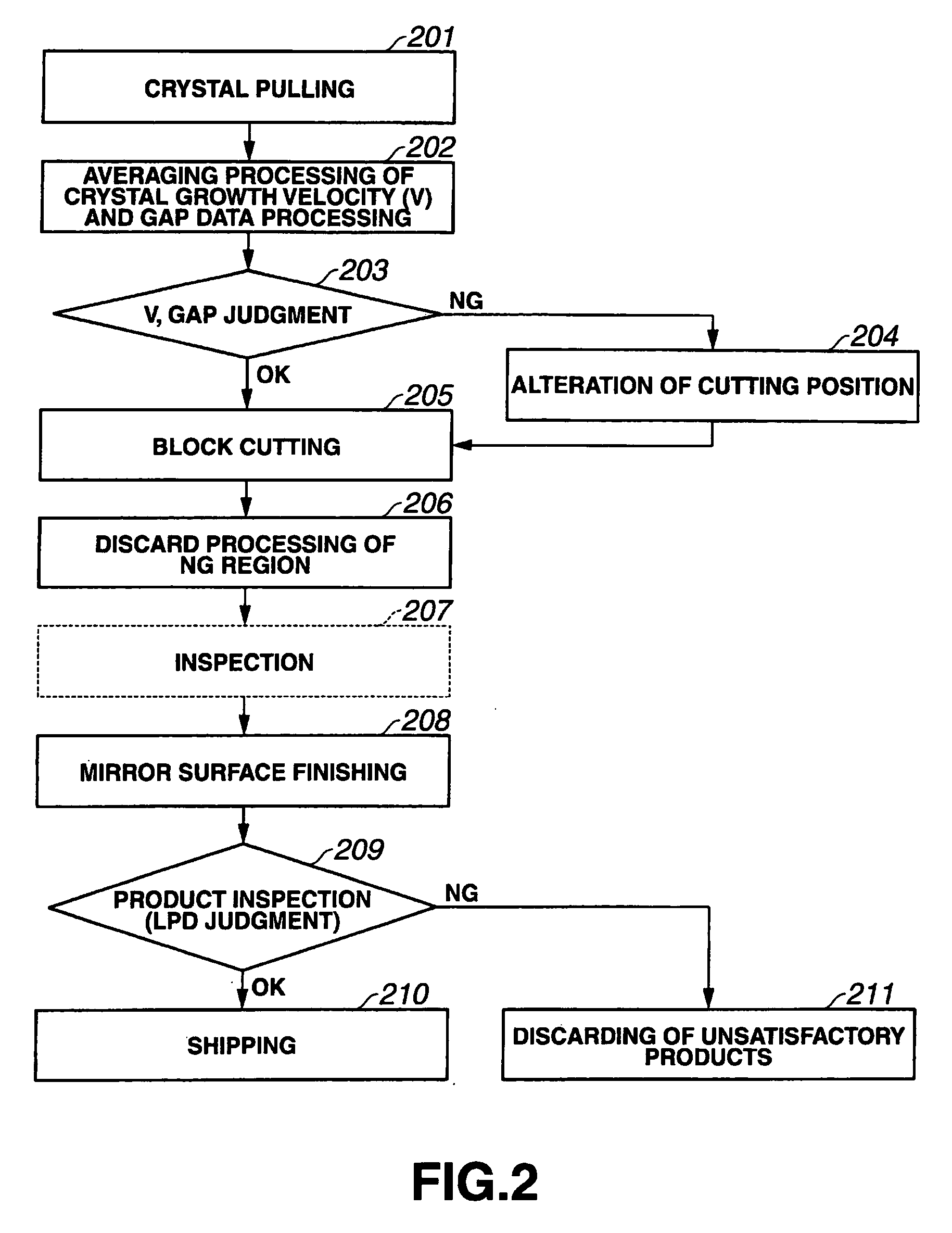
[0023]An embodiment of the present invention will be hereinafter explained with reference to the drawings.

[0024]FIG. 1 is a diagram that shows the configuration of a CZ method silicon single crystal pulling apparatus used in this embodiment. A silicon single crystal pulling apparatus 10 comprises, in the interior of a furnace 11, a crucible 12 for housing a silicon melt 21 that is freely elevatable in the vertical direction and freely rotatable around its elevation axis, a side surface heater 13 provided surrounding the crucible side surface for principally heating the crucible side surface, a base surface heater 14 provided opposing the crucible side surface for principally heating the crucible base surface, and a heat-shielding member 15 provided above the crucible for shielding a silicon single crystal 22 from radiant heat.

[0025]The control parameters applied in this embodiment are “crystal growth velocity V” and a “distance d from a heat-shielding member lower end 15a to a silic...


PUM

PropertyMeasurementUnit
crystal growth velocityaaaaaaaaaa
distanceaaaaaaaaaa
dielectric strengthaaaaaaaaaa

Abstract

In the crystal growth rate (V), there is such a permissible range that the given quality of silicon single crystal can be maintained. This permissible range is determined in advance. The log data of crystal growth rate (V) is measured in the pulling up of silicon single crystal, and using the log data, the actual value of crystal growth rate (V) is determined. The actual value is compared with the permissible range. Any region of silicon single crystal corresponding to crystal growth rate (V) falling within the permissible range is judged as being a conforming region satisfying given standards, while any region of silicon single crystal corresponding to crystal growth rate (V) falling outside the permissible range is judged as being a defective region not satisfying given standards.

Description

TECHNICAL FIELD[0001]The present invention relates to a method of evaluating quality of silicon single crystal in which the quality of a silicon single crystal pulled up from a silicon melt is evaluated, log data of control parameters during crystal growth being employed to evaluate quality across all regions of the crystal.BACKGROUND ART[0002]A demand for higher integration degree and miniaturization of semiconductor devices have arisen in recent years, and this demand has been accompanied by increasingly severe demands in terms of silicon wafer quality. A major characteristic of silicon wafer quality pertains to grown-in defects that appear during growth of the silicon single crystal. Grown-in defects have an undesirable effect during semiconductor device processing on, for example, the dielectric strength and leakage current characteristics of the insulating oxide film, and are a cause of reduced yield. Accordingly, the density of the defects must be reduced or completely removed...

Claims


Application Information

Patent Timeline
Patent Type & Authority Applications(United States)
IPC IPC(8): C30B15/20
CPCC30B15/20C30B15/203C30B29/06
Inventor KOTOOKA, TOSHIROUMATSUKUMA, SHINSAISHOJI, TOSHIAKI
Owner SUMCO TECHXIV
Why Eureka
Try Eureka