
Rigid flexible printed circuit board having openings

a printed circuit board and flexible technology, applied in the field of pcb (printed circuit boards), can solve the problems of difficult to improve the transfer characteristic, difficult to improve the flexibility deterioration of the flexible section, so as to reduce the characteristic impedance of the wire traces, improve flexibility, and minimize the capacitance coupling

Inactive Publication Date: 2007-08-30
SAMSUNG ELECTRONICS CO LTD
View PDF0 Cites 12 Cited by
  • Summary
  • Abstract
  • Description
  • Claims
  • Application Information

AI Technical Summary

Benefits of technology

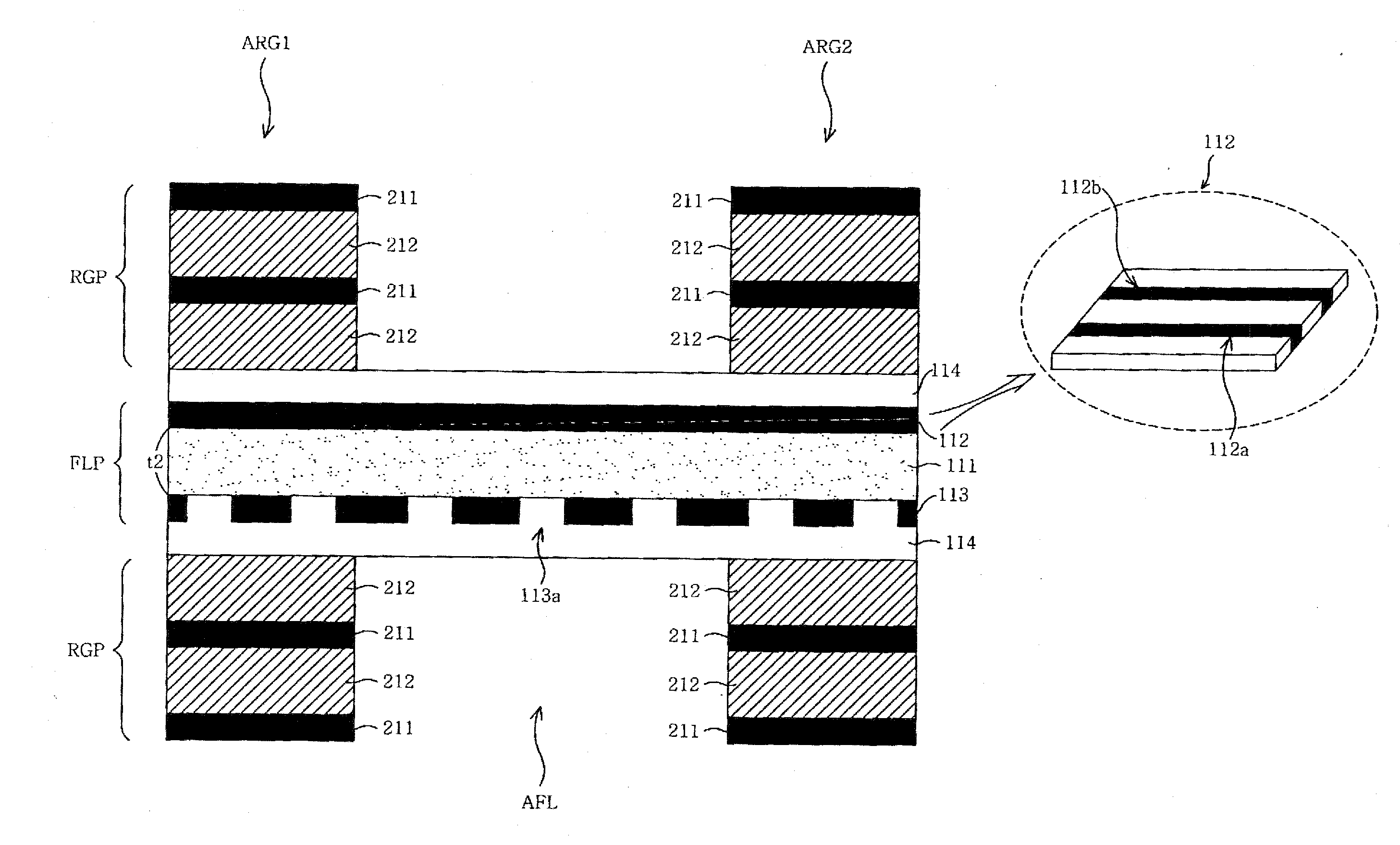
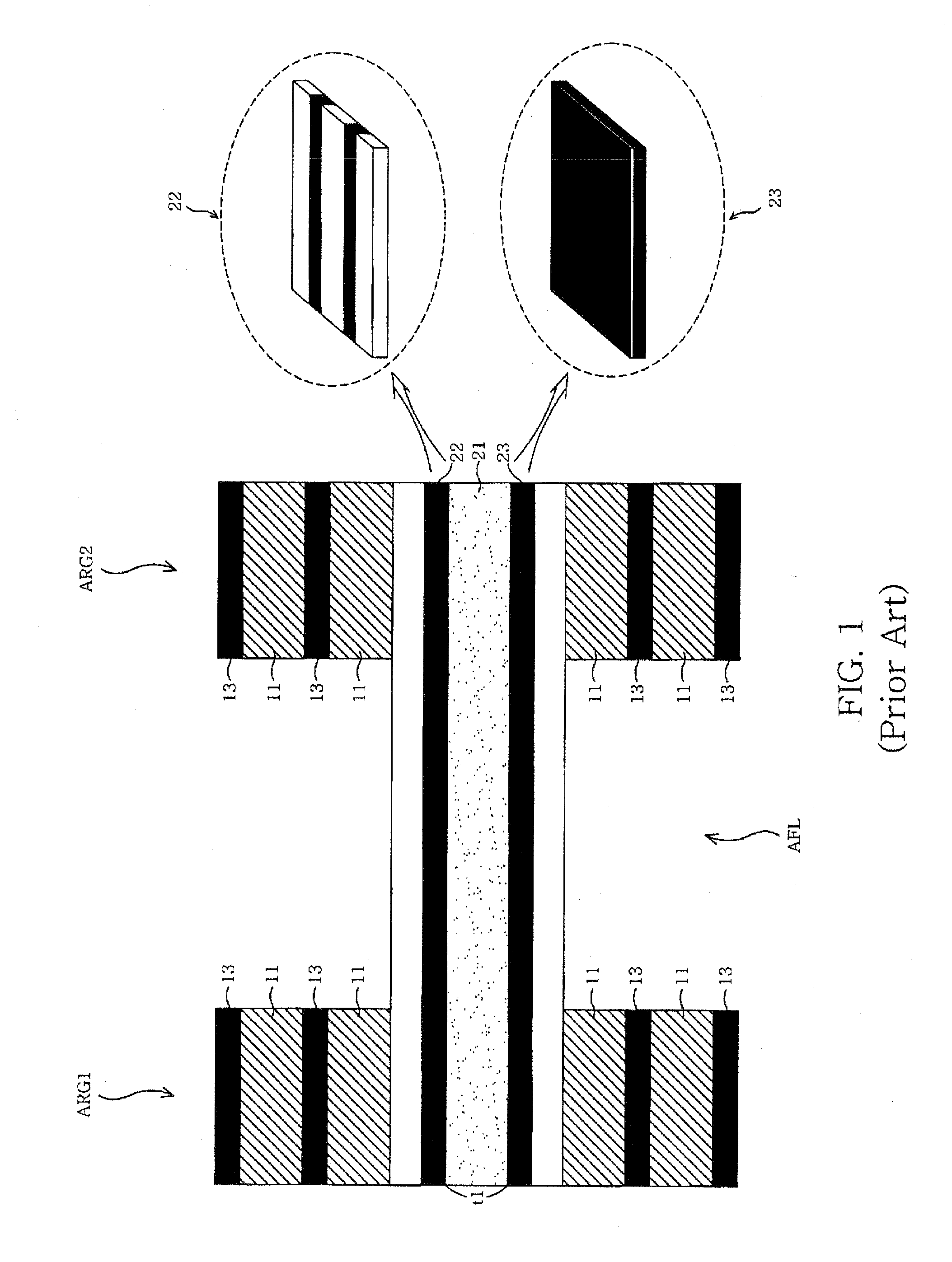
[0010]An object of the invention is to provide a rigid flexible printed circuit board having openings. In order to accomplish the above object, there is provided a rigid flexible printed circuit board. The rigid flexible printed circuit board includes a flexible section and rigid sections being formed at the edge of the flexible section. The flexible section comprises a flexible plane. The flexible plane comprises a base insulating layer; a wire conducting layer being capable of having wire traces to transfer signals between the rigid sections, a wire conducting layer being adhered to one of the top side and the bottom side of the base insulating layer; and a plane conducting layer being adhered to the other of the top side and the bottom side of the base insulating layer, the plane conducting layer for transferring a reference voltage between the rigid sections. The plane conducting layer has a plurality of openings being formed as a mesh structure. The openings minimize the capacitive coupling between the wire conducting layer and the plane conducting layer, thereby decreasing the characteristic impedance of the wire traces while simultaneously allowing for a thin base insulating layer to improve flexibility.

Problems solved by technology

As a result, there is input impedance mismatching between signal wire traces and mounted components, so that it is difficult to improve the transfer characteristic.
However, there is a problem that the flexibility of the flexile section is deteriorated.
Thus, in the conventional rigid flexible PCB, it is difficult to improve flexibility of the flexible section and a characteristic impedance of signal wire traces at the same time.

Method used


Image

  • Rigid flexible printed circuit board having openings
  • Rigid flexible printed circuit board having openings
  • Rigid flexible printed circuit board having openings

Examples


Embodiment Construction

[0017]The invention is described in detail herein by describing preferred embodiments with reference to the accompanying drawings.

[0018]In the drawings, the same reference numerals are used to designate the same or similar components. In the following description, detailed descriptions may be omitted if it is determined that the detailed descriptions of related well-known functions and construction may make the gist of the invention unclear.

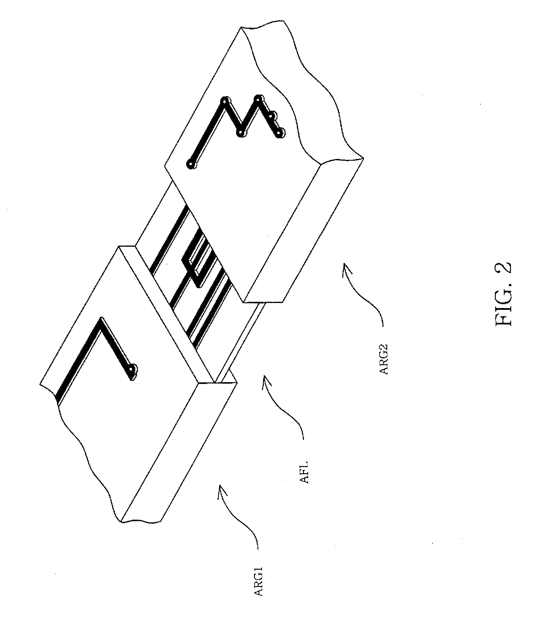
[0019]FIG. 2 is an inclined view showing a rigid flexible PCB according to some embodiments. Referring to FIG. 2, the rigid flexible PCB includes a flexible section AFL and rigid sections ARG1 and ARG2. The rigid sections ARG1 and ARG2 are formed at the edges of the flexible section AFL. The flexible section AFL is flexible, while the rigid sections ARG1 and ARG2 are mechanically stiff. Electrical signals may be transferred between the rigid sections, ARG1 and ARG2, and the flexible section AFL.

[0020]Conductive wire traces may be formed in the fl...


PUM

PropertyMeasurementUnit
flexibleaaaaaaaaaa
voltageaaaaaaaaaa
impedanceaaaaaaaaaa

Abstract

Disclosed herein is a rigid flexible PCB having openings. The rigid flexible PCB includes a flexible section with flexibility and rigid sections being formed at the edges of the flexible section with mechanical stiffness. The flexible section comprises a flexible plane. The flexible plane comprises a base insulating layer; a wire conducting layer being adhered to one of the top side and the bottom side of the base insulating layer; and a plane conducting layer adhered to the other of the top side and the bottom side of the base insulating layer. The plane conducting layer has a plurality of openings being formed as a mesh structure. According to the rigid flexible PCB of the invention, the flexibility of the flexible section and the characteristic impedance of signal wire traces may be improved.

Description

CROSS-REFERENCE TO RELATED APPLICATION[0001]This application claims priority under 35 U.S.C. § 119 from Korean Patent Application No. 2006-18550 filed on Feb. 27, 2006, the contents of which are incorporated herein by reference in their entirety.BACKGROUND[0002]1. Technical Field[0003]The disclosure relates, in general, to a PCB (Printed Circuit Board) and, more particularly, to a Rigid Flexible PCB.[0004]2. Description of the Related Art[0005]A PCB is used for connecting various mounted electrical components with wire traces. In this case, it is very important to match the characteristic impedance of the wire traces with the input impedance of the mounted electrical components. Since the input impedance of the mounted electrical components is designed to be low, the characteristic impedance of the wire traces is desired to be low as well.[0006]Meanwhile, a PCB capable of mounting components with high density is desired, due to the miniaturization of electronic products. According t...

Claims


Application Information

Patent Timeline
Patent Type & Authority Applications(United States)
IPC IPC(8): B32B3/00
CPCH05K1/0224H05K1/0253H05K3/4691Y10T428/24917H05K2201/09681Y10T428/24926H05K2201/09318E02F3/966F15B15/1447F15B21/008
Inventor OH, BYOUNG-HAKIM, JONG-HOON
Owner SAMSUNG ELECTRONICS CO LTD
Learn More