Vertical interconnection circuit structure between substrate-integrated ridge waveguide plates

A technology of substrate integration and circuit structure, applied in circuits, waveguide-type devices, electrical components, etc., can solve the problems of poor mutual isolation, complicated installation process, and large volume of air waveguides.

Active Publication Date: 2018-08-10
10TH RES INST OF CETC
View PDF11 Cites 4 Cited by
  • Summary
  • Abstract
  • Description
  • Claims
  • Application Information

AI Technical Summary

Problems solved by technology

However, the main problems of this structure are: the microstrip probe realizes the waveguide microstrip transition, and additional metal waveguide short-circuit surface structures are required, which increases the circuit volume and weight; the air waveguide is too large, especially in the millimeter wave frequency band. Realization of high-density integration; the entire transition structure contains more than one circuit element, which requires a secondary hybrid integration process to achieve
[0005] The rapid development of miniature millimeter-wave connectors also provides a solution for the interconnection between millimeter-wave boards. The smaller and smaller high-frequency connectors such as SSMP and WMP can realize the vertical interconnection between boards of millimeter-wave circuits, but there are the following problems: The use of micro connectors to realize the vertical interconnection between millimeter-wave boards actually requires two high-frequency connectors and dual female (KK) connectors installed on the substrate to achieve. Although this method can achieve blind insertion and has a certain three-dimensional off-axis redundancy However, the volume of the overall interconnection structure is still relatively large compared to the requirements for high-density integration in the millimeter wave band; the interconnection structure requires two high-frequency connectors and a KK connector, and the high-frequency connectors need to be installed on the Substrate surface, poor integration, complex installation process, high cost for mass use
However, due to its open layout, the transmission and mutual isolation of the millimeter-wave frequency band are not good. The final connection between the two boards needs to be realized through high-temperature melting of BGA balls, which increases the temperature gradient of the entire component assembly and easily leads to bare chips. Secondary pollution, and substrate thermal stress, solder joint fracture, etc. will bring a series of long-term reliability problems

Method used


Image

  • Vertical interconnection circuit structure between substrate-integrated ridge waveguide plates
  • Vertical interconnection circuit structure between substrate-integrated ridge waveguide plates

Examples


Embodiment Construction

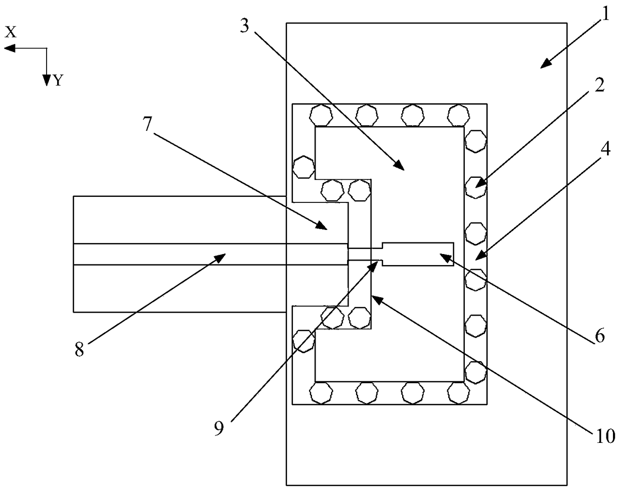
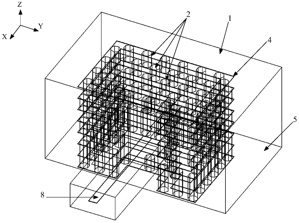
[0017] refer to figure 1 with figure 2 . In the embodiment described below, a substrate-integrated ridge waveguide interconnection circuit structure includes two LTCC multilayer circuit boards 1 with the same conversion circuit structure, and the SIRW 3 interface is metal-etched on the surface of the substrate. The Z-direction metallized filling hole 2 equivalently constitutes the waveguide wall of SIRW 3 and the single-sided equivalent dielectric waveguide ridge 10 in the waveguide, the waveguide short-circuit surface 5, and the 50-ohm stripline 8 and stripline 8 that are matched and connected through the high-resistance stripline 9. A linear probe 6, wherein: on the LTCC multilayer circuit board 1, a SIRW3 ​​perpendicular to the surface of the substrate is integrated, and a substrate integrated ridge waveguide opening is etched on the corresponding exit of the metal ground on the surface of the LTCC multilayer circuit board 1; Z direction The metallized filling hole 2 is ...


PUM


Abstract

The invention provides an inter-board perpendicular interconnection circuit structure for a substrate integrated ridge waveguide (SIRW), and aims to provide a millimeter wave inter-board perpendicular interconnection circuit structure with small volume, easy integration, high interconnection property and long-term reliability. The inter-board perpendicular interconnection circuit structure is implemented by the following technical scheme: the SIRW (3) perpendicular to the surface of a base board is integrated on an LTCC multilayered circuit board (1); a substrate integrated ridge waveguide opening is etched in a corresponding outlet in the metal ground on the surface of the LTCC multilayered circuit board (1); Z-direction metalized filling holes (2) are arranged to form a metal hole gate array to equivalently form the waveguide wall and single-side ridges in the waveguide; metallic shield holes and probe restraining cavities (7) on the two sides of a 50-ohm strip line (8) are arranged at the equal spacing; and the alignment pressing and connection of the SIRW interfaces on the opposite sides between two boards is realized through pin hole alignment, so that the perpendicular interconnection transition of the millimeter wave signal between two boards in a way of 50-ohm strip line-SIRW-SIRW-50-ohm strip line is realized consequently.

Description

technical field [0001] The invention relates to a vertical interconnection circuit structure between boards based on a Z-direction substrate integrated ridge waveguide (Substrate-Integrated-Ridge-Waveguide, SIRW). Background technique [0002] With the rapid development and wide application of millimeter wave technology, higher and higher requirements are put forward for the miniaturization, multi-function and high integration of millimeter wave components. In response to the above requirements, there are usually two technical approaches for chip-level primary integration and secondary integration of multi-functional substrates, and the corresponding integration architecture has gradually changed from the previous two-dimensional plane integration to three-dimensional stacking integration. The first chip-level integration can use semiconductor technology such as TSV and Flipchip to complete the stacking of multiple chips and the interconnection of high and low frequency sign...

Claims


Application Information

Patent Timeline
Patent Type & Authority Patents(China)
IPC IPC(8): H01P5/00H01P5/08
CPCH01P5/00H01P5/08
Inventor 张凯黄建
Owner 10TH RES INST OF CETC
Why Eureka
Try Eureka