Semiconductor light-emitting device

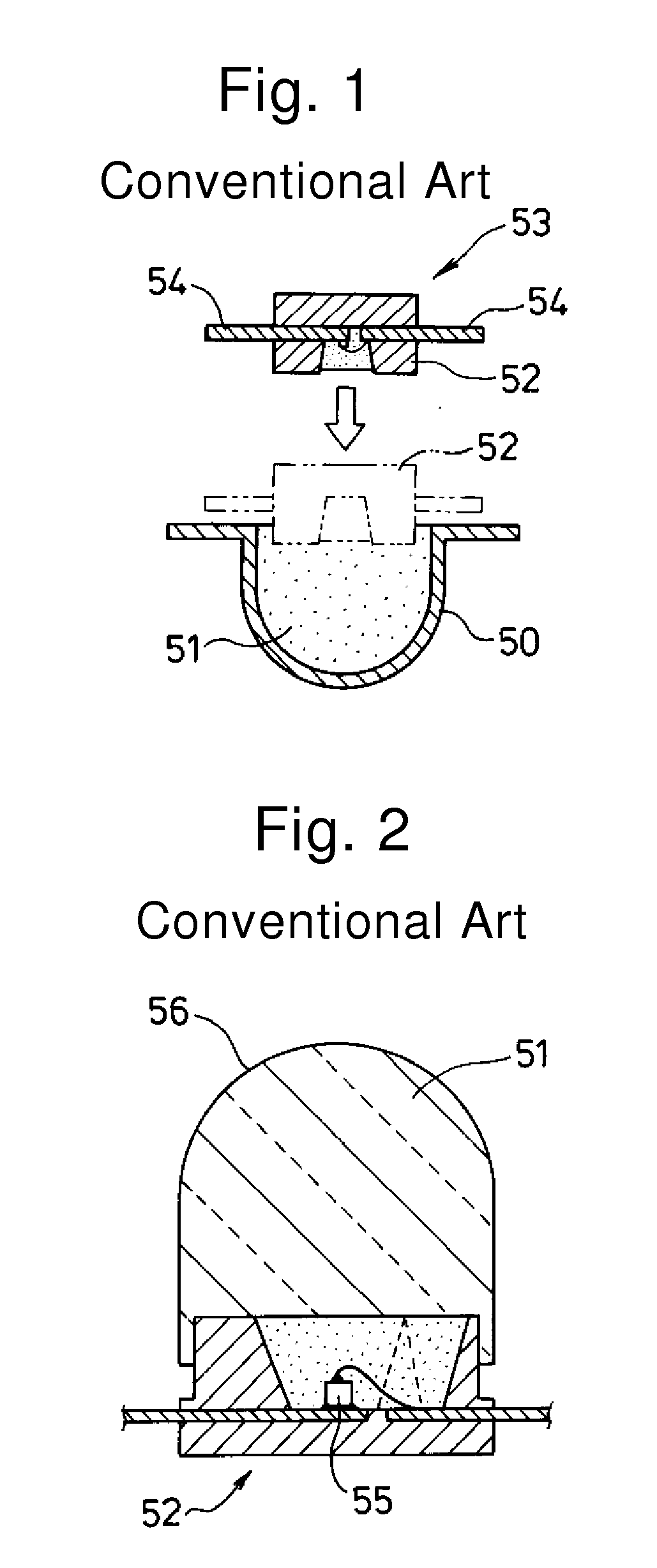
a technology of semiconductors and light-emitting devices, which is applied in the direction of semiconductor devices, basic electric elements, electrical appliances, etc., can solve the problems of inability to achieve the same light gathering efficiency, the size and height of the surface mount light-emitting devices is subject to the constraint that the size and height of the device should be small, and the inability to secure the lens diameter and the adequate distance between the led chip and the lens, as provided in the cannon-ball type led

Inactive Publication Date: 2007-09-06
STANLEY ELECTRIC CO LTD
View PDF10 Cites 98 Cited by
  • Summary
  • Abstract
  • Description
  • Claims
  • Application Information

AI Technical Summary

Benefits of technology

[0041] The soft resin spacer serves as a thermal stress relaxation layer provided between the semiconductor light-emitting element-mounted body and the optical lens which are integrated together. The thermal stress relaxation layer can provide several different effects, including the prevention of peeling caused by thermal stresses at the time of environmental temperature changes (the peeling typically occurring at the interfaces between the components). Thus, a semiconductor light-emitting device having a high reliability and high light extraction efficiency can be realized.

Problems solved by technology

Meanwhile, the surface mount light-emitting devices are subjected to the constraint that the size and height thereof should be small, which is one of the aspects of these types of LEDs.
Hence, even when the resin-encapsulated portion is formed into a lens shape, an adequate distance between the LED chip and the lens and an adequate lens diameter as provided in the cannon-ball type LED often cannot be secured.
Therefore, the attained light gathering efficiency is sometimes not comparable to that of the cannon-ball type LEDs, and the difficulty lies in achieving an axial luminous intensity comparable to that of the cannon-ball type LEDs.
However, in the light-emitting device constituted as described above, each of the components forming the interfaces is repeatedly subjected to thermal expansion and contraction caused by environmental temperature changes.
However, when the thermal expansion coefficients of these materials are different from each other, a difference occurs in the amount of thermal expansion or contraction between the components, which generates stresses associated with the difference.
Hence, the possibility arises that peeling occurs at the interface, especially when there is no chemical bonding at the interface.
In particular, interfacial peeling tends to occur when the interface is formed from high hardness materials.
In time, this leads to the deterioration of optical characteristics of a light-emitting device (such as the reduction in luminous intensity), and thus the reliability of the product is also impaired.

Method used


Image

  • Semiconductor light-emitting device
  • Semiconductor light-emitting device
  • Semiconductor light-emitting device

Examples


Embodiment Construction

[0057] Exemplary embodiments of the presently disclosed subject matter will be described in detail with reference to FIGS. 3 to 12. The exemplary embodiments described hereinafter are specific examples of the disclosed subject matter, and thus various technical features and characteristics are added thereto. However, the scope of the present invention of the disclosed subject matter is not limited to the exemplary embodiments.

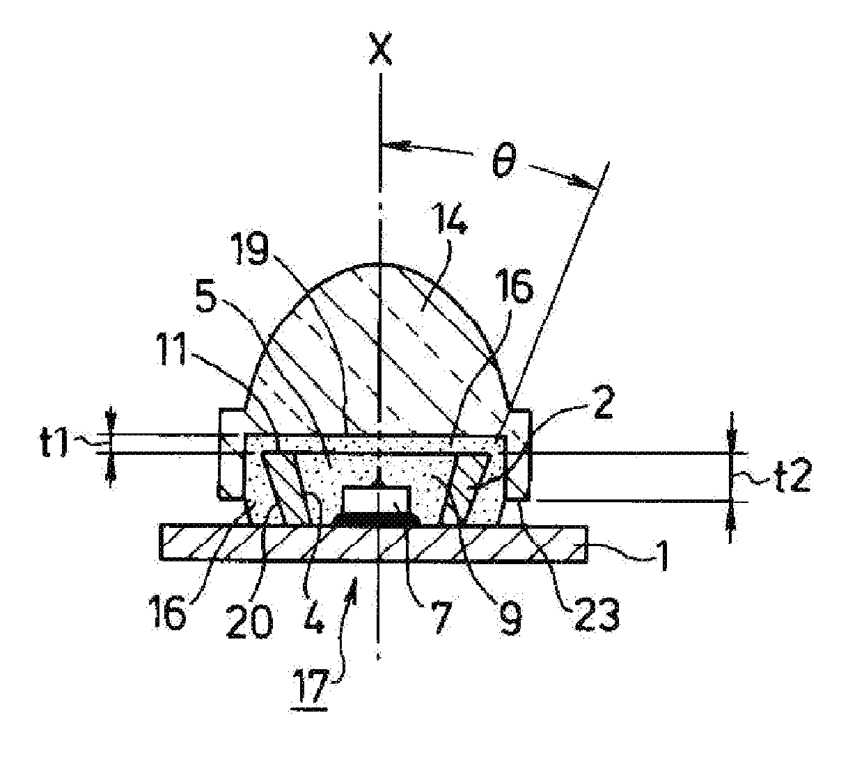
[0058] A semiconductor light-emitting device made in accordance with principles of the disclosed subject matter can be configured to include a semiconductor light-emitting element-mounted body, an optical lens, and a transparent soft resin spacer.

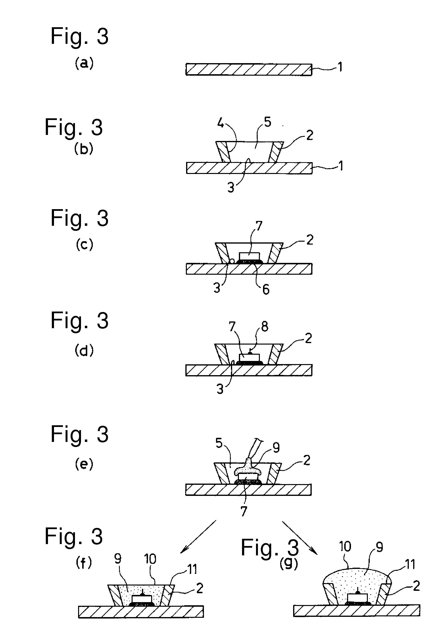
[0059] The semiconductor light-emitting element-mounted body is one of the components of the semiconductor light-emitting device, and first the manufacturing steps thereof are described with reference to FIGS. 3(a)-(g).

[0060] In FIG. 3(a) a circuit substrate 1 on which electrode wiring has been preformed can be prov...


PUM


Abstract

In a conventional semiconductor light-emitting device having a semiconductor light-emitting element-mounted body and an optical lens which are located adjacent each other, interfacial peeling sometimes occurs at the contact interfaces between components when the device is subjected to outside temperature changes. This may lead to the deterioration of optical characteristics and the reduction in reliability of the device. In accordance with an aspect of the disclosed subject matter, a semiconductor light-emitting element-mounted body can be integrated with the optical lens via a soft resin spacer. Hence, the soft resin spacer can serve as a thermal stress relaxation layer located between the semiconductor light-emitting element-mounted body and the optical lens, which are integrated together. The thermal stress relaxation layer can possibly prevent peeling, caused by thermal stresses due to outside temperature changes, from occurring at the interfaces between the components.

Description

[0001] This application claims the priority benefit under 35 U.S.C. § 119 of Japanese Patent Application No. 2005-260772 filed on Sep. 8, 2005, which is hereby incorporated in its entirety by reference. [0002] 1. Technical Field [0003] The presently disclosed subject matter relates to a semiconductor light-emitting device, and in particular to a semiconductor light-emitting device which employs a semiconductor light-emitting element as a light source and has a unit for converting the wavelength of light. [0004] 2. Description of the Related Art [0005] Examples of light-emitting devices, which employ a semiconductor light-emitting element as a light source, include LED light-emitting devices which employ a light emitting diode (LED) as a semiconductor light-emitting element. Such light-emitting devices are broadly categorized into two types, i.e., a vertical light-emitting device and a surface mount light-emitting device, according to their external shapes and the mounting methods th...

Claims


Application Information

Patent Timeline
Patent Type & Authority Applications(United States)
IPC IPC(8): H01L33/00H01L33/58H01L33/50H01L33/60
CPCH01L33/52H01L33/58H01L2224/48091H01L2224/48247H01L2224/48465H01L2224/73265H01L2924/00014H01L2924/00
Inventor HARADA, MITSUNORI
Owner STANLEY ELECTRIC CO LTD
Why Eureka
Try Eureka