Current sensing circuit

a current sensing circuit and current sensing technology, applied in the direction of resistance/reactance/impedence, pulse technique, instruments, etc., can solve the problems of inability to achieve prior art solutions, inability to find negative rails, inaccuracy of current measurement, etc., to achieve efficient sensing of current flowing through the transistor, efficient detecting load current through load

Active Publication Date: 2007-09-06
INFINEON TECH AG
View PDF13 Cites 183 Cited by
  • Summary
  • Abstract
  • Description
  • Claims
  • Application Information

AI Technical Summary

Benefits of technology

[0012] One or more aspects of the invention provide a circuit arrangement for efficiently detecting a load current through a load.
[0013] One...

Problems solved by technology

By employing this principle the prior art solutions often do not overcome either the constraint of not having a negative supply rail or the problem that the current flowing in the larger device might have the opposite direction than the current flowing in the replica or in a part of the replicas.
Apart from having additional circuitry the problem is that often no negative rail is available.
Moreover, matching issues involving both transistors and resistors may occur and the sensing resistor Rsense introduces a voltage difference in the gate voltage that results in current measurement inaccuracies.
However, the current sensing circuit shown in FIG. 2...

Method used


Image

  • Current sensing circuit
  • Current sensing circuit
  • Current sensing circuit

Examples


first embodiment

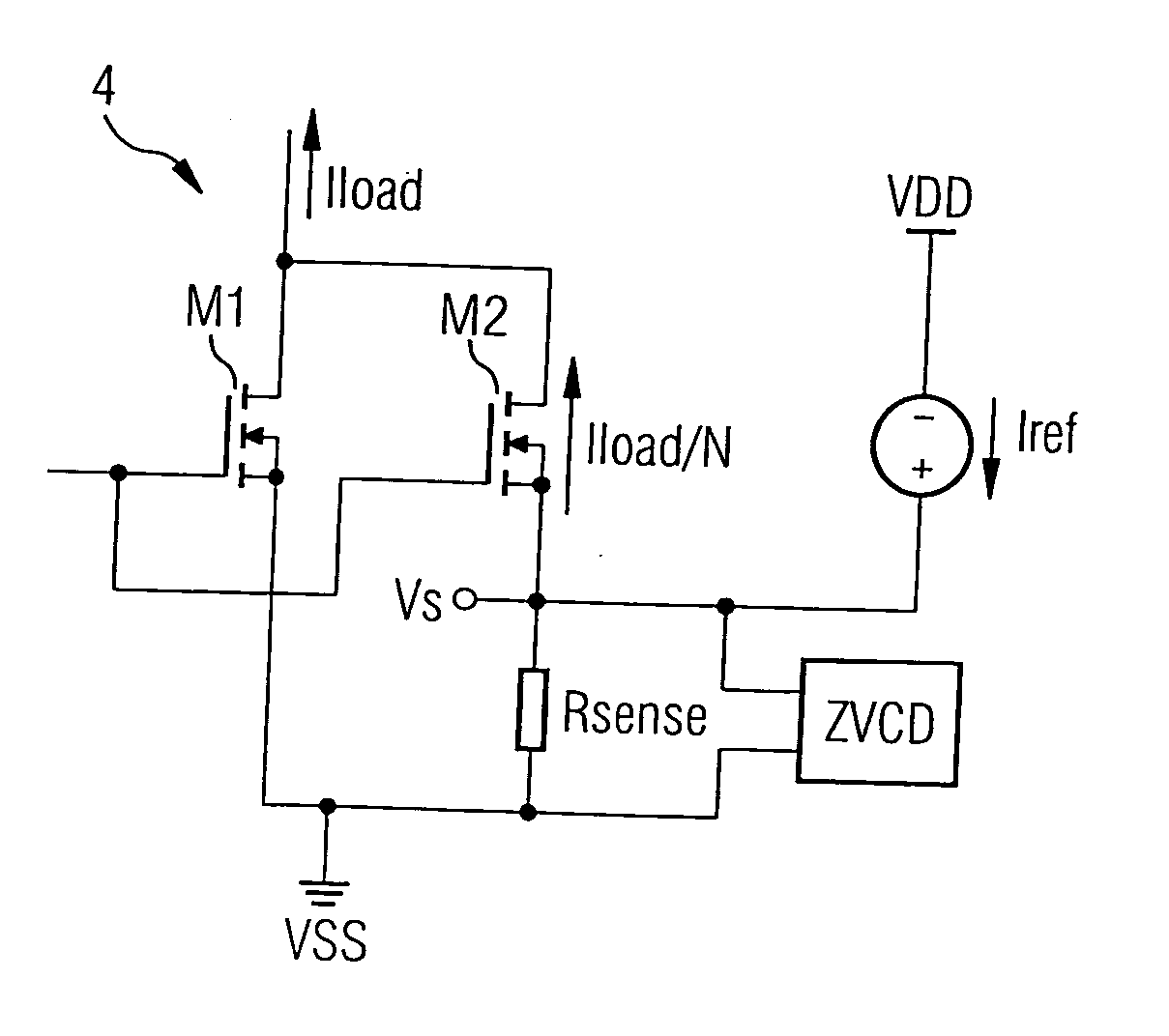
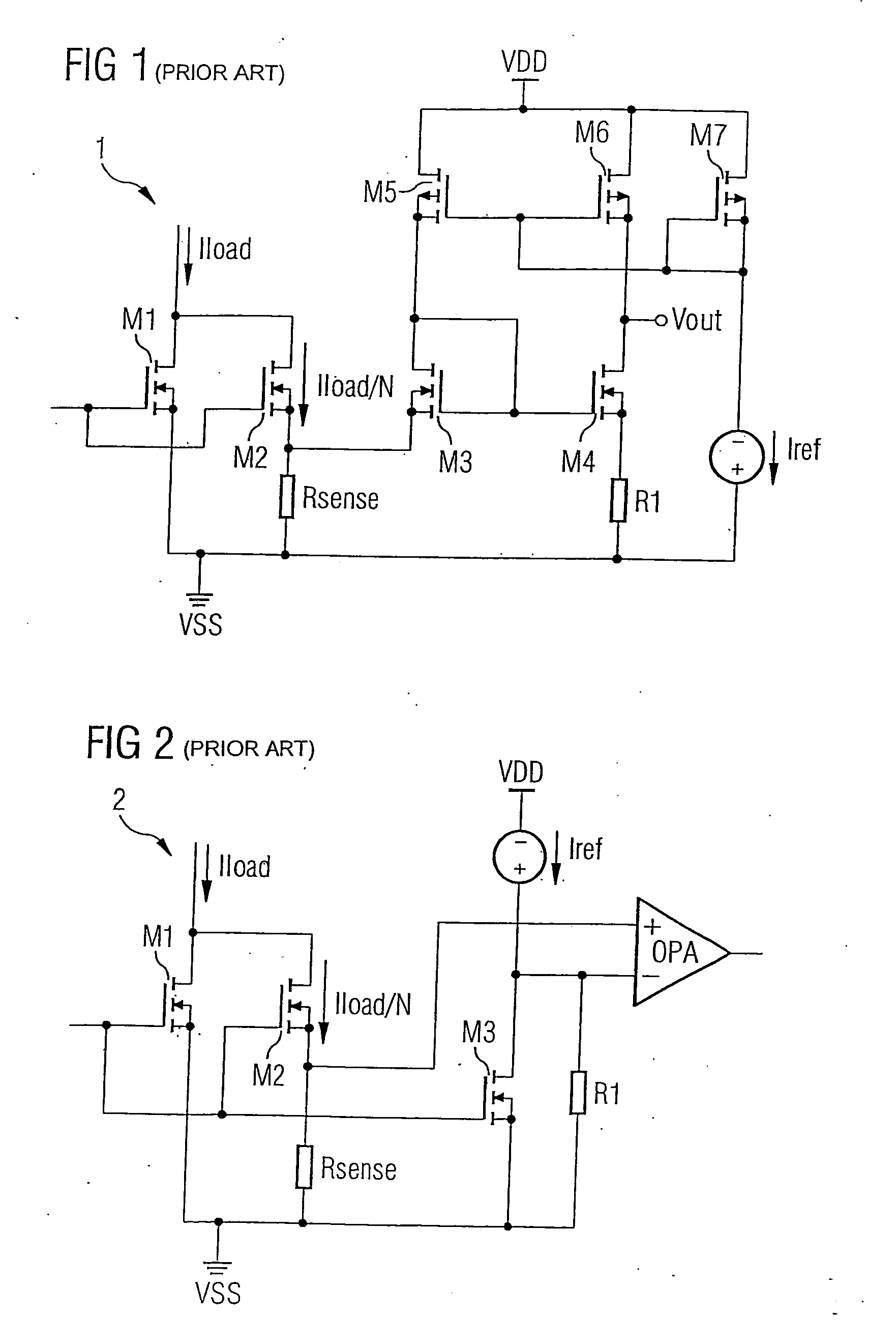
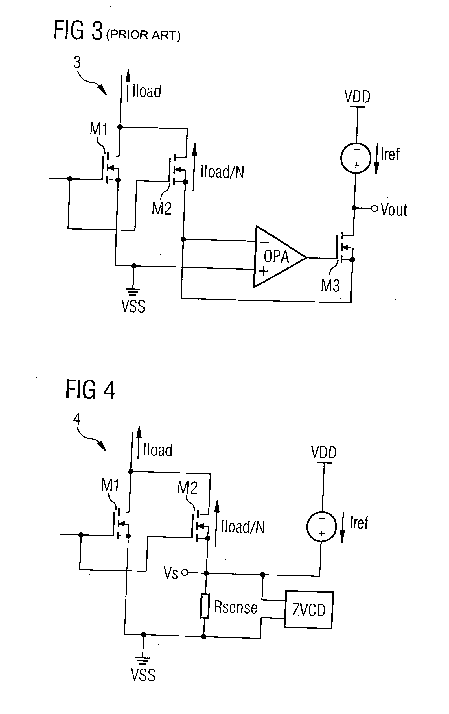
[0034] In FIG. 4 the circuit arrangement according to the invention is designated by the reference numeral 4. In this embodiment of the circuit arrangement according to the invention, a main transistor M1 and a sensing transistor M2 are provided. Both transistors M1 and M2 are n-channel MOS transistors and are interconnected on their drain sides. Furthermore, the control terminal of the sensing transistor M2 is connected to the control terminal of the main transistor M1. The load path of the main transistor M1 is connected in series with the load, which is not shown in FIG. 4. A load current Iload flows through the load path of the main transistor M1. Since the area (or the width) of the sensing transistor M2 has a value which is a fraction 1 / N of the area (or the width) of the main transistor M1, a scaled current Iload / N flows through the load path of the sensing transistor M2. The area (or the width) of the main transistor M1 is much larger than the area (or the width) of the sens...

second embodiment

[0040] In FIG. 5 the circuit arrangement according to the invention is designated by the reference numeral 5. In contrast to the circuit arrangement 4 shown in FIG. 4, FIG. 5 shows how the inventive concept can be implemented into a high-side switch. In FIG. 5 the same elements as in FIG. 4 are provided with the same reference symbols.

[0041] In the circuit arrangement 5 the main transistor M1 and the sensing transistor M2 are p-channel MOS transistors. The control terminal of the sensing transistor M2 is connected to the control terminal of the main transistor M1. The load path of the main transistor M1 is connected in series with the load, which is not shown in FIG. 5. A load current Iload flows through the load path of the main transistor M1. Since the width (or the area) of the sensing transistor M2 has a value which is a fraction 1 / N of the width (or the area) of the main transistor M1, a scaled current Iload / N flows through the load path of the sensing transistor M2. The factor...

third embodiment

[0044] In FIG. 6 the circuit arrangement according to the invention is designated by the reference numeral 6. The circuit arrangement 6 is a buck converter comprising the circuit arrangement 5 shown in FIG. 5. As can be seen from FIG. 6, the supply potential VDDb being higher than the supply potential VDD is in this example obtained by bootstrapping the switching node.


PUM


Abstract

A circuit arrangement for detecting a load current through a load includes a main transistor, a sensing transistor through which a load current flows that is a measure of the load current flowing through the main transistor, a means of resistance which is connected in series with the load path of the sensing transistor, a current source which is connected to a node which is arranged between the sensing transistor and the means of resistance, and a detector which detects the load current flowing through the main transistor by measuring the voltage across the means of resistance.

Description

FIELD OF THE INVENTION [0001] The present invention relates generally to a current sensing circuit and method, and more particularly to a circuit for detecting a load current through an integrated switch. BACKGROUND OF THE INVENTION [0002] Many applications and implementations that employ integrated switches, such as integrated switched mode power converters, may require that the current flowing through the switches is monitored or compared with given reference values. The reasons for this are related either to regulation or control aspects or to the implementation of additionally required features, such as many kinds of current limitation circuits. [0003] The adopted solutions suitable for silicon integration found so far are always based on the combination of the real switch device carrying the current of interest with a smaller replica or replicas of the switch itself. Typically the real switch device is an integrated MOS transistor through which the load current flows. The switc...

Claims


Application Information

Patent Timeline
IPC IPC(8): G01R27/08
CPCG01R19/0092H03K17/687H03K17/18
Inventor FABBRO, SIMONENORLING, KARLLINDHOLM, CHRISTIAN
Owner INFINEON TECH AG
Why Eureka
Try Eureka