Probeless DC testing of CMOS I/O circuits

a technology of cmos and i/o circuits, applied in the field of semiconductor testing, to achieve the effect of small siz

Inactive Publication Date: 2007-09-06
DIALOG SEMICONDUCTOR GMBH
View PDF14 Cites 29 Cited by
  • Summary
  • Abstract
  • Description
  • Claims
  • Application Information

AI Technical Summary

Problems solved by technology

The probing of the small I / O pads of an integrated circuit chip by a tester exposes the I / O pad to damage, which creates problems for electrically connecting the I / O pads to the next higher level of assembly.

Method used


Image

  • Probeless DC testing of CMOS I/O circuits
  • Probeless DC testing of CMOS I/O circuits
  • Probeless DC testing of CMOS I/O circuits

Examples


Embodiment Construction

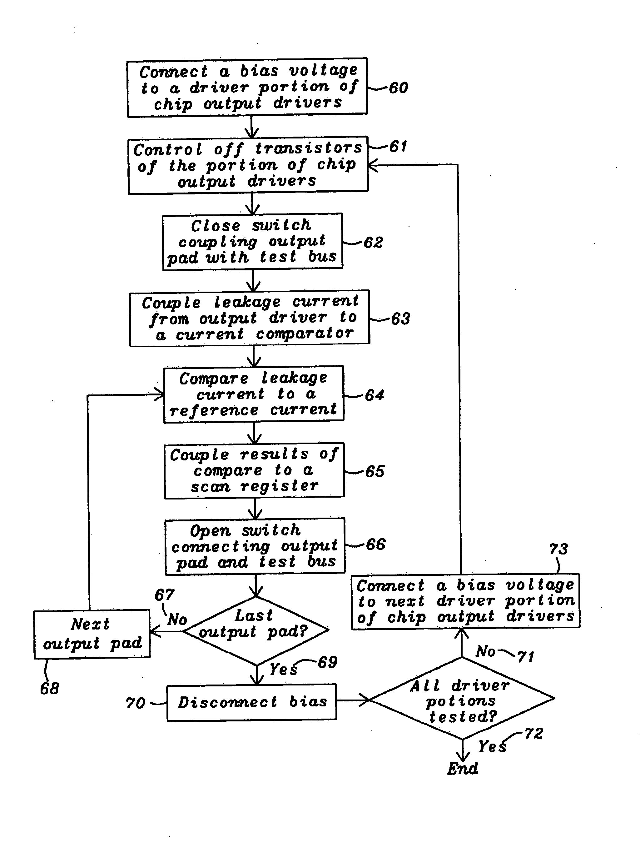
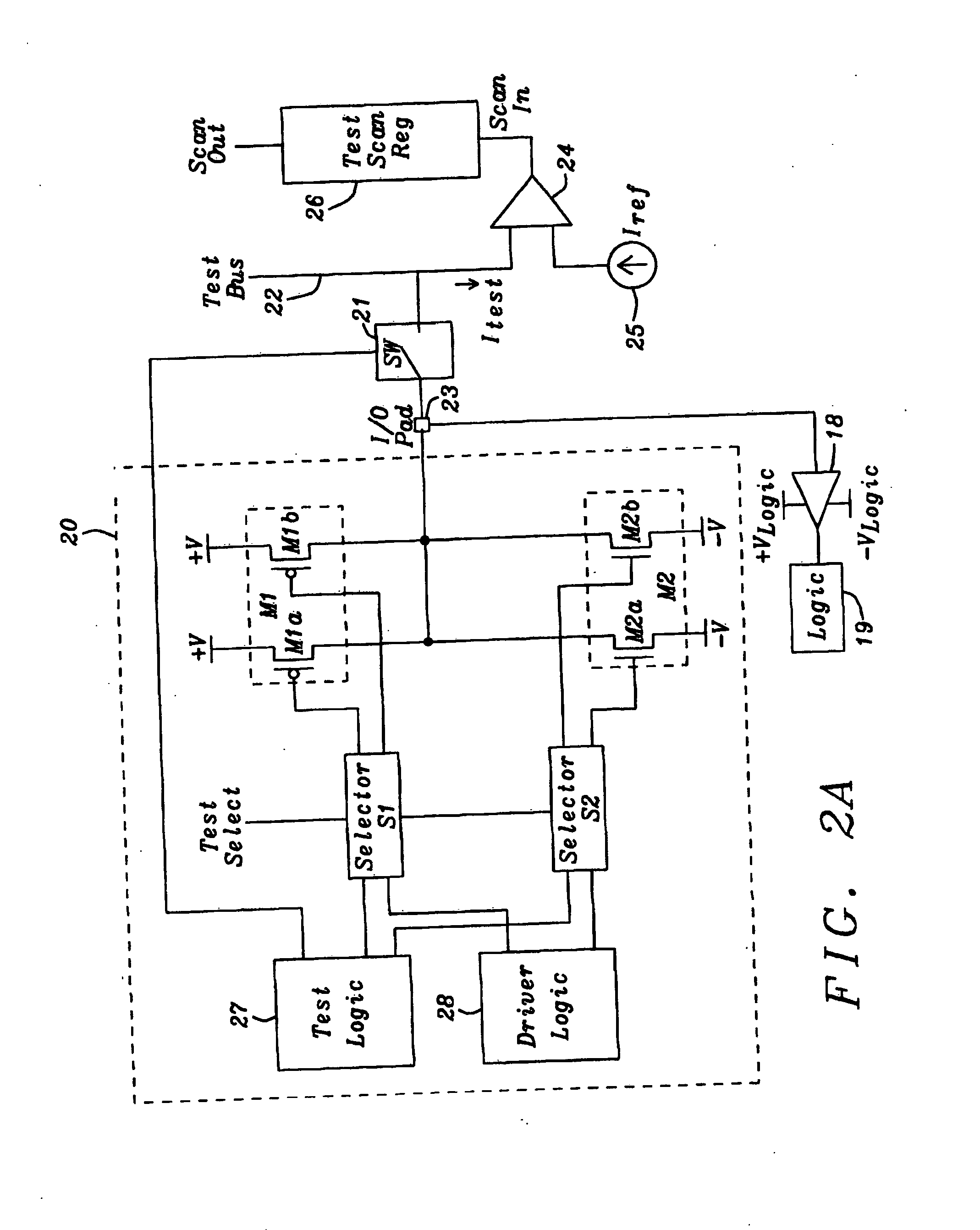
[0035] In FIG. 2A is shown a circuit diagram of an I / O receiver circuit 18 coupled to logic circuits 19 and an output driver circuit 20 coupled to an I / O pad 23. The output driver circuit 20 is coupled by a switch 21 to a test bus 22. The output driver 20 comprises a P-channel transistor M1 and an N-channel transistor M2. The control gates of transistors M1 and M2 are segmented into a plurality of control gate portions forming a plurality of transistors sharing the same transistor device channel. For simplicity of explanation the segmentation of the transistors M1 and M2 is assumed to be two portions. Thus, the control gate of M1 is shown to be segmented into two portions forming transistor M1a and M1b, in like manner the control gate of M2 is shown to be segmented into two portions forming transistors M2a and M2b. By definition herein transistors M1b and M2b are test transistors, and M1b and M2b have a gate area that is a fraction of the total gate area of M1a plus M1b and M2aplus ...


PUM


Abstract

A method and implementation is described by which I / O input and output circuitry of a CMOS chip are measured without the need to probe the chip. Output driver transistors are used to provide marginal voltages to test input circuits, and the output driver transistors are segmented into portions where a first portion is used to provide a representative “on” current, which is coupled to a test bus that is further connected to a current comparator circuit contained within the chip. Both leakage and “on” current of the driver transistors is measured using segmented driver transistors. The output of the current comparator circuit is connected to a test scan register or to a test output from which test results are obtained digitally. The testing techniques are also applicable for other semiconductor devices.

Description

TECHNICAL FIELD [0001] The present invention is related to semiconductor testing, and in particular to testing CMOS I / O drivers. BACKGROUND ART [0002] As the integration of semiconductor chips continues, smaller and smaller geometries have occurred with more and more I / O circuits included to reduce the number of chips needed to implement a function. With the onset of advancement in displays creating LCD screens and other methods of display, the need for testing the ability of the I / O drive circuits to perform a specified function is necessary to guarantee the quality of the drivers. Driver leakage current testing as well as drive current capability is crucial to guarantee a quality display to insure segment and common connections to a display create a quality image. [0003] A paper title “Verification and Auto Test for LCD Driver / Controller”, Zhuo et al., Proceedings 5th International Conference on ASIC, October 2003, Vol.: 2, pp.: 1175-1178 is directed to two methods that fulfill th...

Claims


Application Information

Patent Timeline
Patent Type & Authority Applications(United States)
IPC IPC(8): G01R31/26
CPCG01R31/2884G01R31/318569G01R31/3161
Inventor STAUDT, HANS MARTIN VOSCOFFEY, TONY
Owner DIALOG SEMICONDUCTOR GMBH
Why Eureka
Try Eureka