

Method for forming layer for trench isolation structure
- Summary
- Abstract
- Description
- Claims
- Application Information
AI Technical Summary
Benefits of technology
Problems solved by technology
Method used
Image

Examples
Embodiment Construction
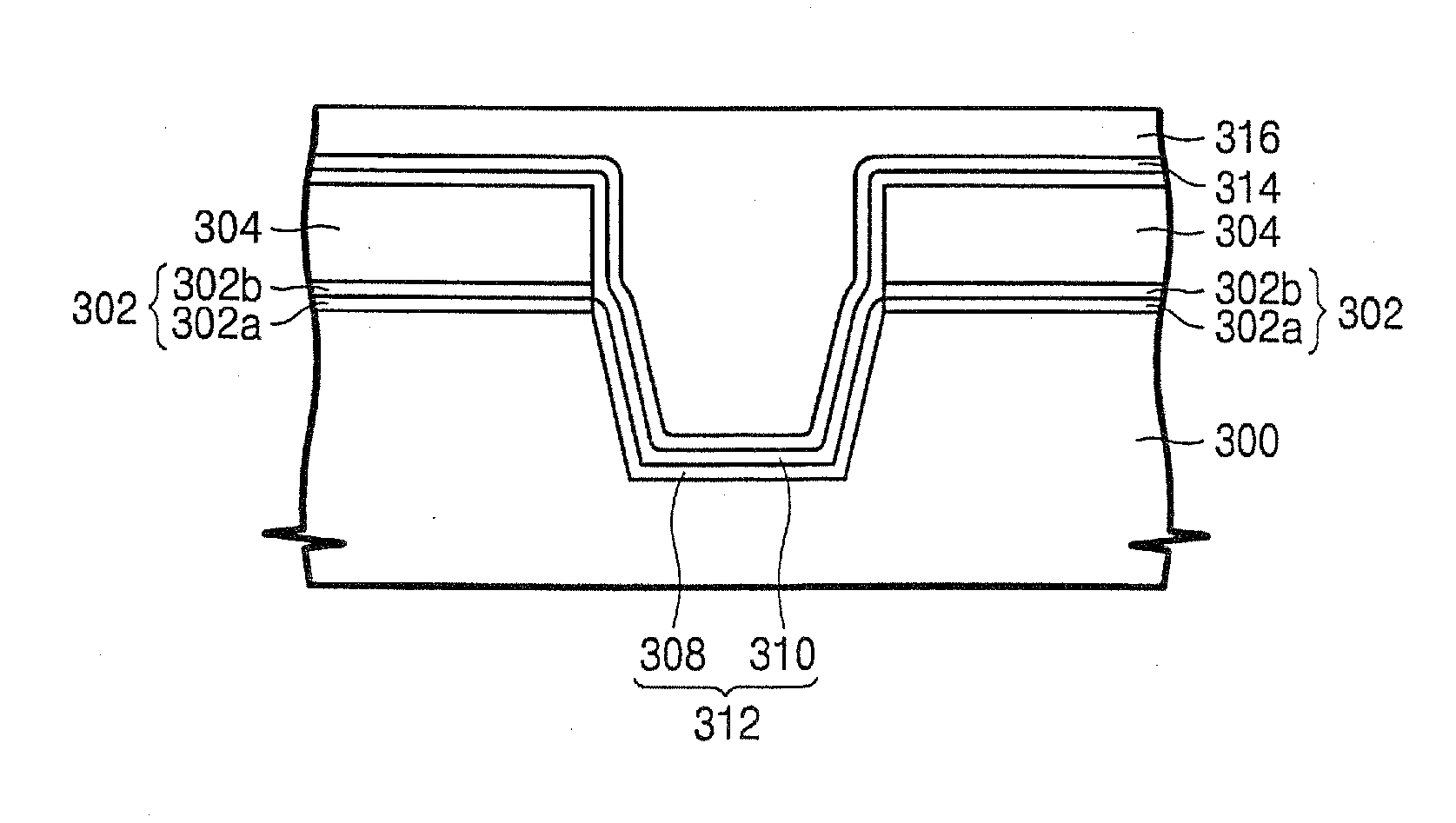
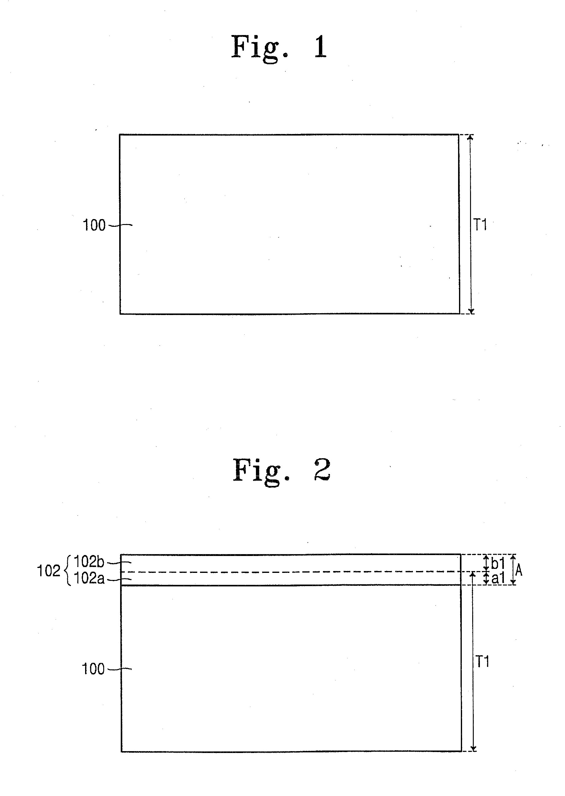
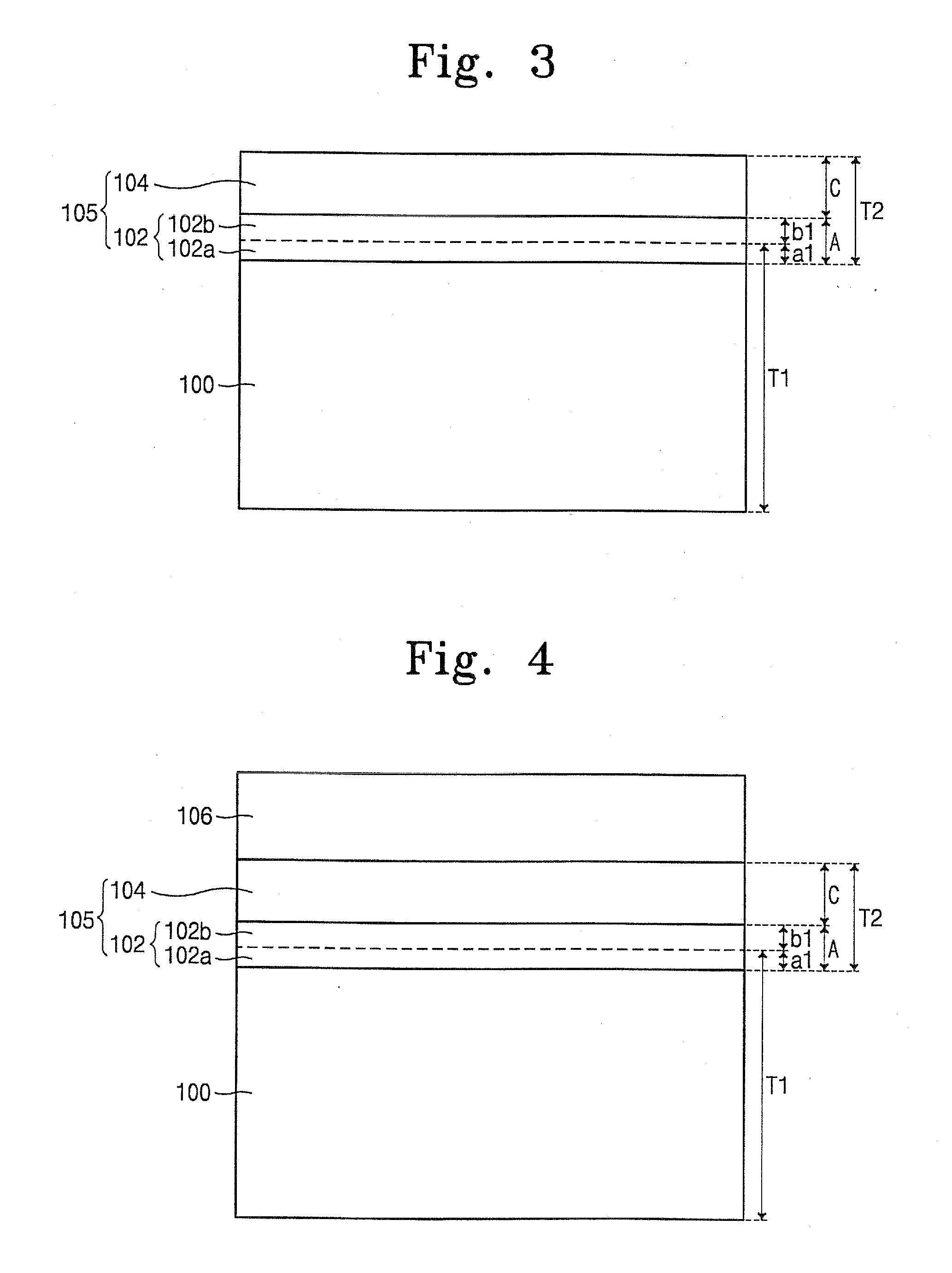
[0028] In order to solve the above-mentioned problems encountered in the prior art, the present invention employs a dual layer of a thermal oxide layer and a CVD oxide layer (or other insulating layer) formed thereon.
[0029]FIG. 1 illustrates a cross-sectional view of a semiconductor substrate, for example, single crystalline silicon substrate 100 having a thickness of ‘T1’. The silicon substrate 100 may be an exposed single crystalline substrate prior to formation of a thermal oxide layer in various semiconductor fabrication processes, for example: a single crystalline silicon substrate prior to formation of a pad oxide layer (thermal oxide layer); a single crystalline silicon substrate following device isolation and prior to formation of a thermal oxide layer acting as an ion-implanting buffer layer; a single crystalline silicon substrate prior to the formation of a gate dielectric layer, and a single crystalline silicon substrate following gate etching and prior to a thermal oxid...
PUM
 Abstract
Description
Claims
Application Information