Power semiconductor device

Active Publication Date: 2007-09-20
HITACHI LTD
View PDF4 Cites 200 Cited by
  • Summary
  • Abstract
  • Description
  • Claims
  • Application Information

AI Technical Summary

Benefits of technology

[0009]A power semiconductor device of the present invention is capable of achieving high blocking vo

Problems solved by technology

In JP-A-10-56131, though an IGBT module was achieved with a flip chip structure to enhance heat radiation, because a high heat-conductivity insulating resin, in stead of metal, was mounted on and under the module, there was limitation in reduction of thermal resistance, and further a study on a structure f

Method used


Image

  • Power semiconductor device
  • Power semiconductor device
  • Power semiconductor device

Examples


Example

Embodiment 1

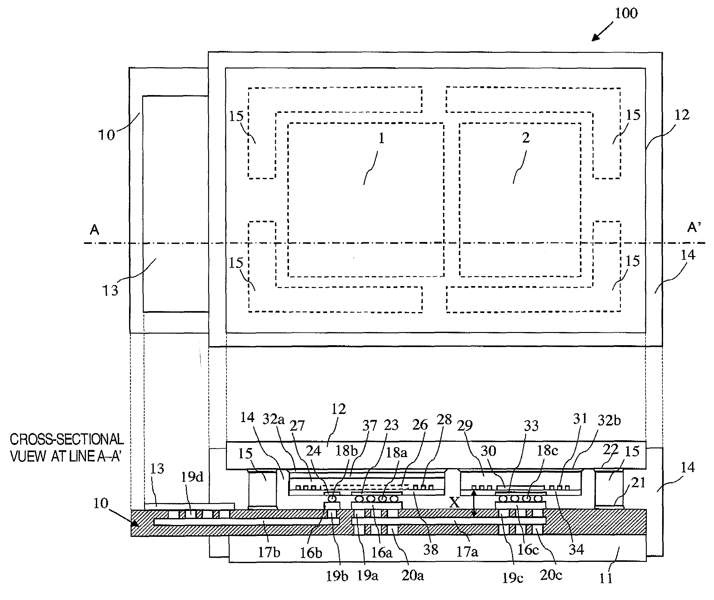
[0036]FIG. 1 is a plan and cross-sectional view of a power semiconductor device of the present embodiment. The present embodiment is one for the case where a power transistor such as an IGBT, a power MOSFET and a wide band-gap JFET, and a diode 2 are surface mounted as a unit. In the present embodiment, a power semiconductor device has a p-type emitter region 26 (though an emitter diffused layer is a n-type, because it is formed inside a p-type well region, and both of them are in an electrical short-circuit state, hereinafter the region including both of them, is described as the p-type emitter region 26) joined with an emitter electrode of the IGBT 1, and an n-type high resistance region 27 joined with a collector electrode via a p-type collector region 37, directly joined; in the n-type high resistance region 27, a triple p-type floating field ring 28 is mounted; this triple p-type floating field ring 28 works as a high blocking voltage ensuring region to keep blockin...

Example

Embodiment 2

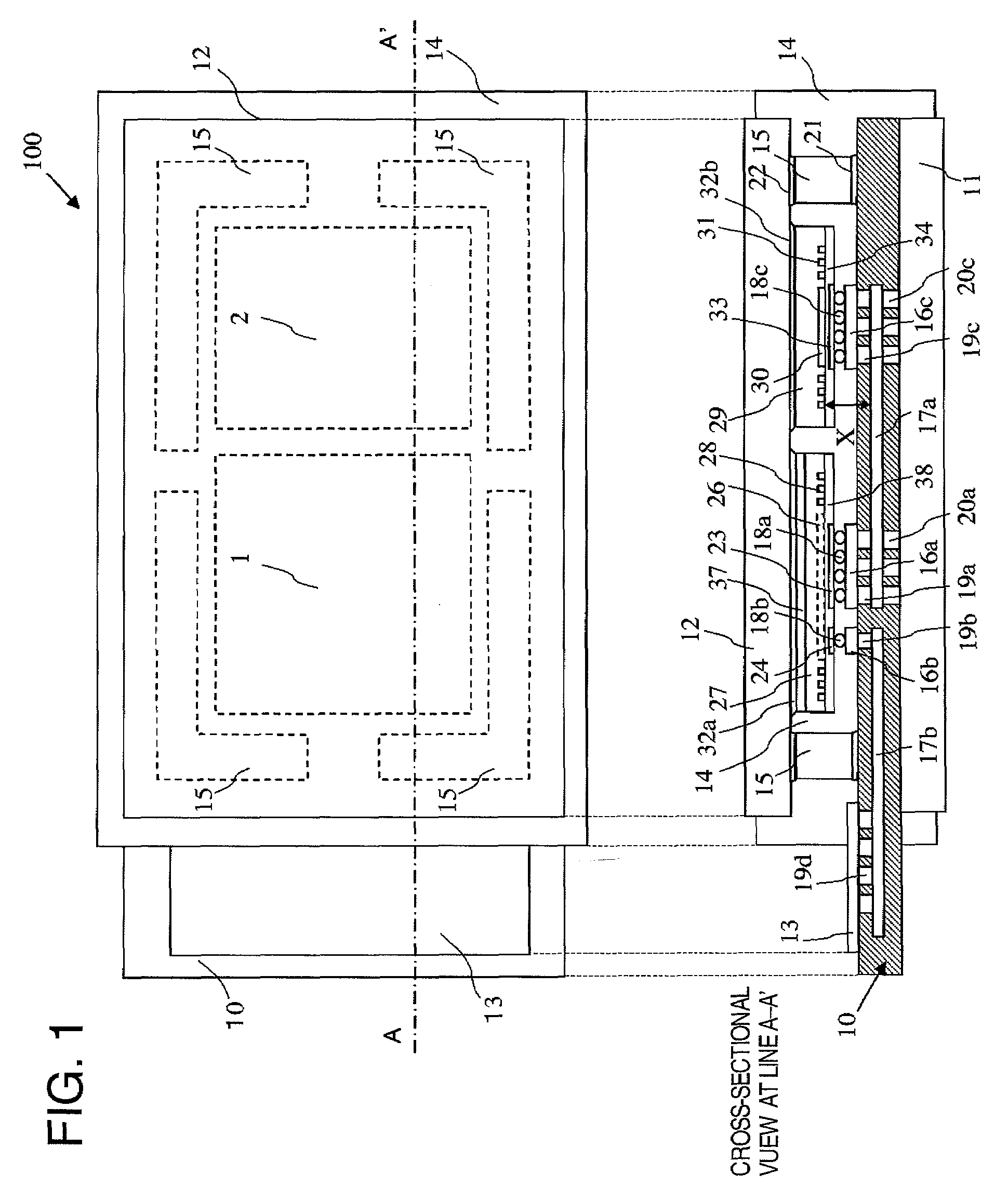
[0048]FIG. 2 is a plan and cross-sectional view of a power semiconductor device of the present embodiment. In the present embodiment, the support materials 15 shown in FIG. 1 are also mounted with a bump of a conductive bonding material 34 and the first electrode wiring layer 16, like in the semiconductor chip such as the IGBT 1 and the diode 2, to make the rate of thermal expansion in the upward and downward directions equal to that of the semiconductor chip such as the IGBT 1 or the diode 2. As other structures are similar to those of Embodiment 1, the similar effect is accomplished.

Example

Embodiment 3

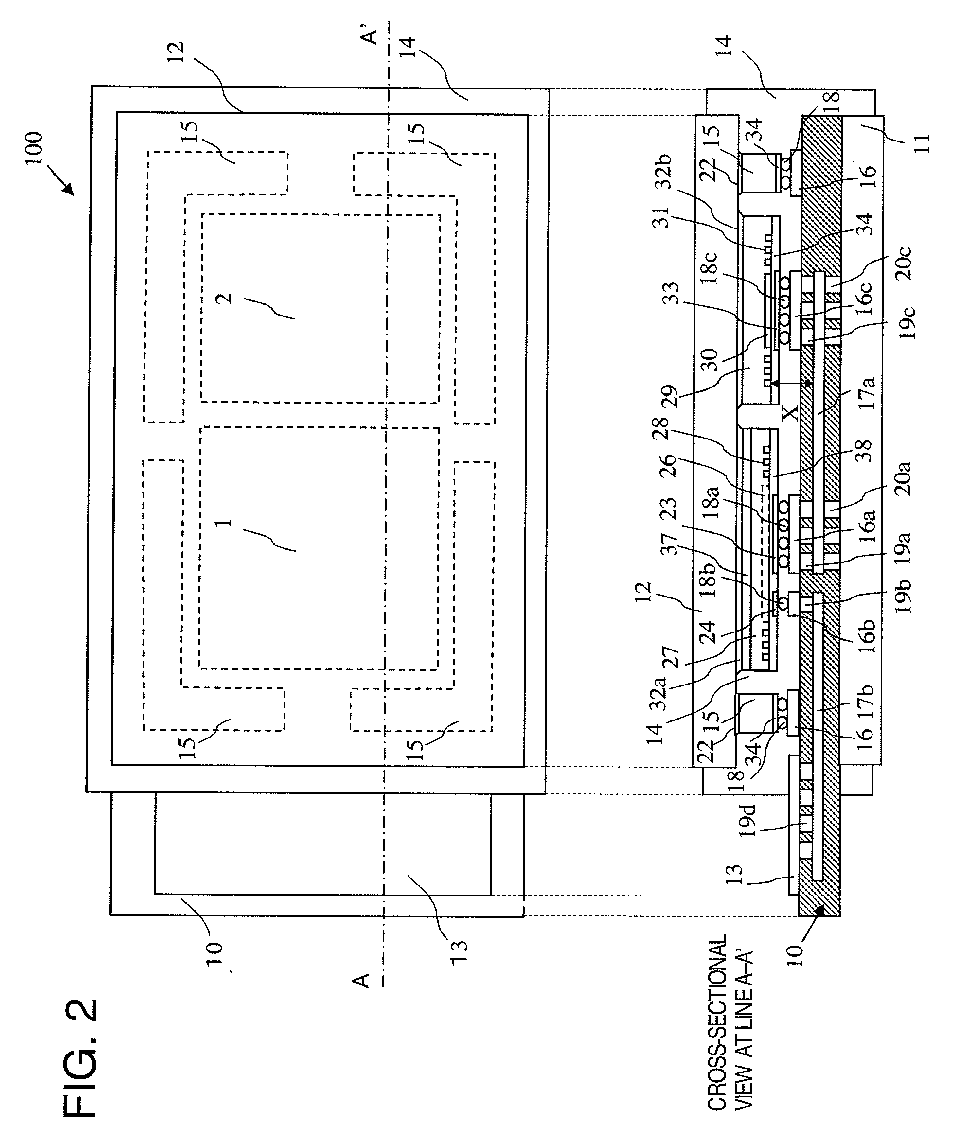
[0049]FIG. 3 is a plan and cross-sectional view of a power semiconductor device of the present embodiment. This embodiment is the case where the high heat-conductivity insulating material resin 14 shown in FIG. 1 is sealed only at the inside of the support materials 15, and because the region to be sealed becomes smaller, compact size can be achieved. As other structures are similar to those of Embodiment 1, the similar effect is accomplished.


PUM


Abstract

A power semiconductor device, having a first semiconductor region, and a second semiconductor region; mounted with a first electrode pad on a semiconductor substrate main surface at the inside surrounded by the third semiconductor region, mounted in the second semiconductor region, and a multilayer substrate having first and second wiring layers, to take out an electrode of the semiconductor chip; joining the first wiring layer part for the first electrode, mounted on the multilayer substrate, in a region opposing to the semiconductor substrate main surface at the inside surrounded by the third semiconductor region, and the first electrode pad, by a conductive material; joining the first wiring layer part for the first electrode, and the second wiring layer at a conductive part; and extending the second wiring layer to the outside of a region opposing the semiconductor substrate main surface at the inside surrounded by the third semiconductor region.

Description

BACKGROUND OF THE INVENTION[0001]The present invention relates to a power semiconductor device, and in particular, relates to a power semiconductor device having high blocking voltage, low thermal resistance, low parasitic resistance, and compact size, and enabling high current performance.[0002]For the purpose of enabling low thermal resistance, low parasitic resistance, compact size, and high current performance, a flip chip structure has been developed, wherein a semiconductor chip is joined to a multilayer substrate not by a wiring, but by a bump or solder. JP-A-10-56131 (description in paragraphs (0020) to (0039)) discloses a semiconductor device, wherein a semiconductor chip is sandwiched between high heat-conductivity insulating substrates, along with an electrode of a semiconductor chip and an electrode pattern of high heat-conductivity insulating substrate are joined by soldering, so as to reduce electric resistance and thermal resistance. Further, it is disclosed that a re...

Claims


Application Information

Patent Timeline
IPC IPC(8): H01L31/00
CPCH01L23/49844H01L2924/13062H01L23/5385H01L25/072H01L25/115H01L25/117H01L2924/10272H01L2924/1033H01L2924/13055H01L2924/13091H01L2924/3011H01L23/5383H01L2924/1305H01L2224/73253H01L2924/15192H01L2924/1301H01L2224/16225H01L2924/00H01L2224/05571H01L2224/05573H01L2924/00014H01L2224/05599
Inventor SAKAMOTO, KOZOISHII, TOSHIAKI
Owner HITACHI LTD
Why Eureka
Try Eureka