Semiconductor wafer thinning

a technology of semiconductor wafers and thinning strips, applied in the field of microelectronics, can solve the problems of difficult processing, thinning of semiconductor wafers, and risks of damaging the integrated circuit supported by the semiconductor wafer, and achieve the effect of avoiding any risk of stress or contamination

Inactive Publication Date: 2007-09-20
STMICROELECTRONICS SRL
View PDF8 Cites 81 Cited by
  • Summary
  • Abstract
  • Description
  • Claims
  • Application Information

AI Technical Summary

Benefits of technology

[0020] In particular, the embodiments ease the implementation of such a thinning by using techniques compatible with those used for the manufacturing of electronic circuits on the wafer.
[0022] In certain embodiments, the present invention also avoids any risk of stress or contamination of the components formed in the semiconductor wafer.

Problems solved by technology

However, the thinning of semiconductor wafers poses several problems.
A first problem is that, if a wafer is thinned down before manufacturing of the components and circuits, it becomes difficult to handle for subsequent processings due to its fragility.
Further, the separation of an adhesive tape is generally performed by tearing, generating risks of damaging the integrated circuits supported by the semiconductor wafer.
Further, the adhesive used to stick the tape on the semiconductor wafer risks generating contaminations in the active wafer areas and certain processings are not compatible with the use of an adhesive tape, due to risks of pollution by degassing of these components.
Further, possible surface unevennesses of the semiconductor wafer may generate a rupture of the wafer due to the mechanical stress in the thinning (especially in case of a grinding rectification).
The use of such a glue of complex composition is likely to pose problems of contamination of the active areas of the circuits supported by the semiconductor wafer.
Further, its application and the subsequent gluing and separation steps require a dedicated equipment.
Such a method substantially exhibits the same disadvantages as the use of an adhesive tape and further requires a high-temperature anneal due to the use of a wax.
Such anneals are noxious for the components formed in the wafer, especially transistors, by creating stress likely to cause breakages or to generate dopant diffusions resulting in malfunctions.

Method used


Image

  • Semiconductor wafer thinning
  • Semiconductor wafer thinning
  • Semiconductor wafer thinning

Examples


Embodiment Construction

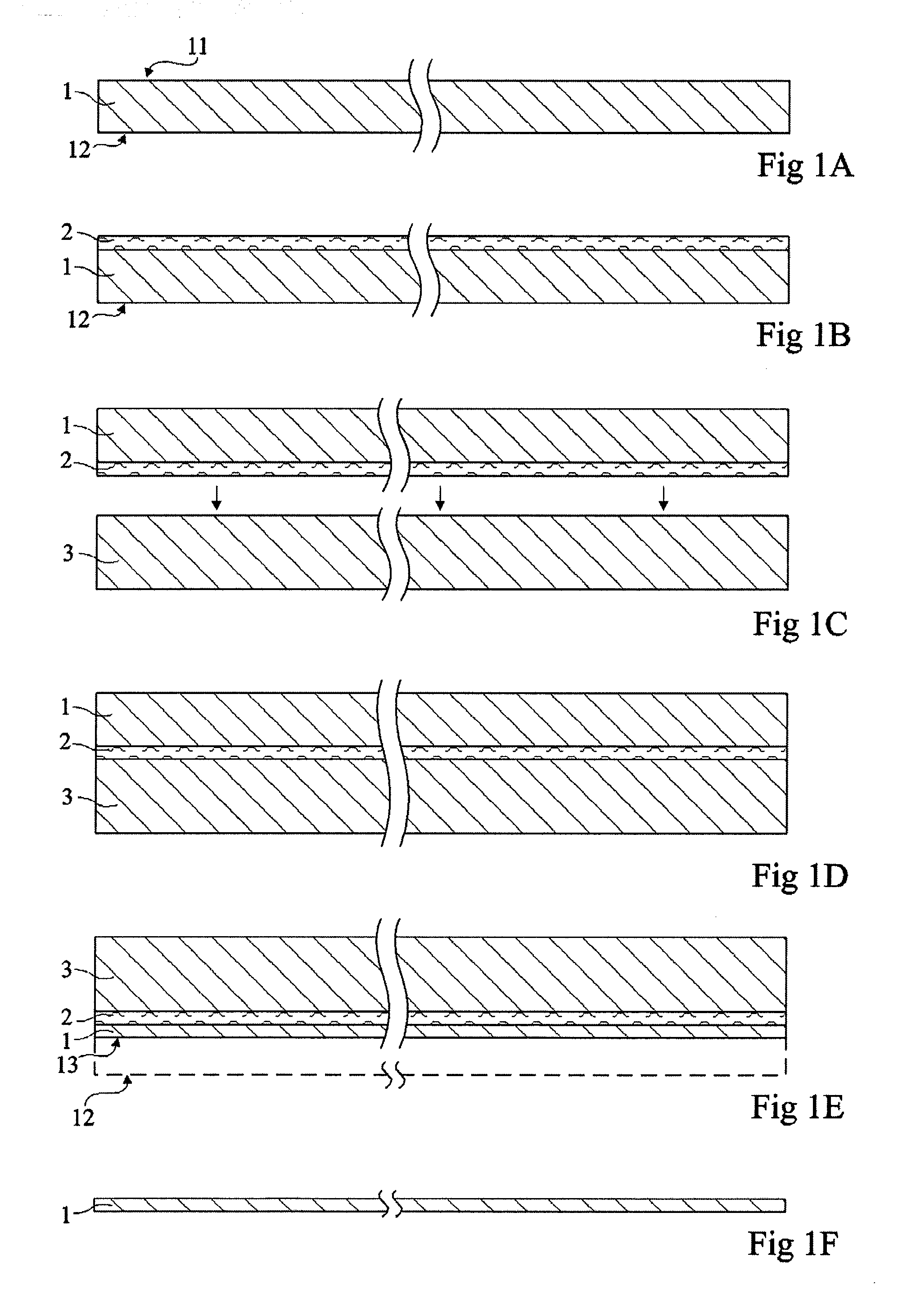
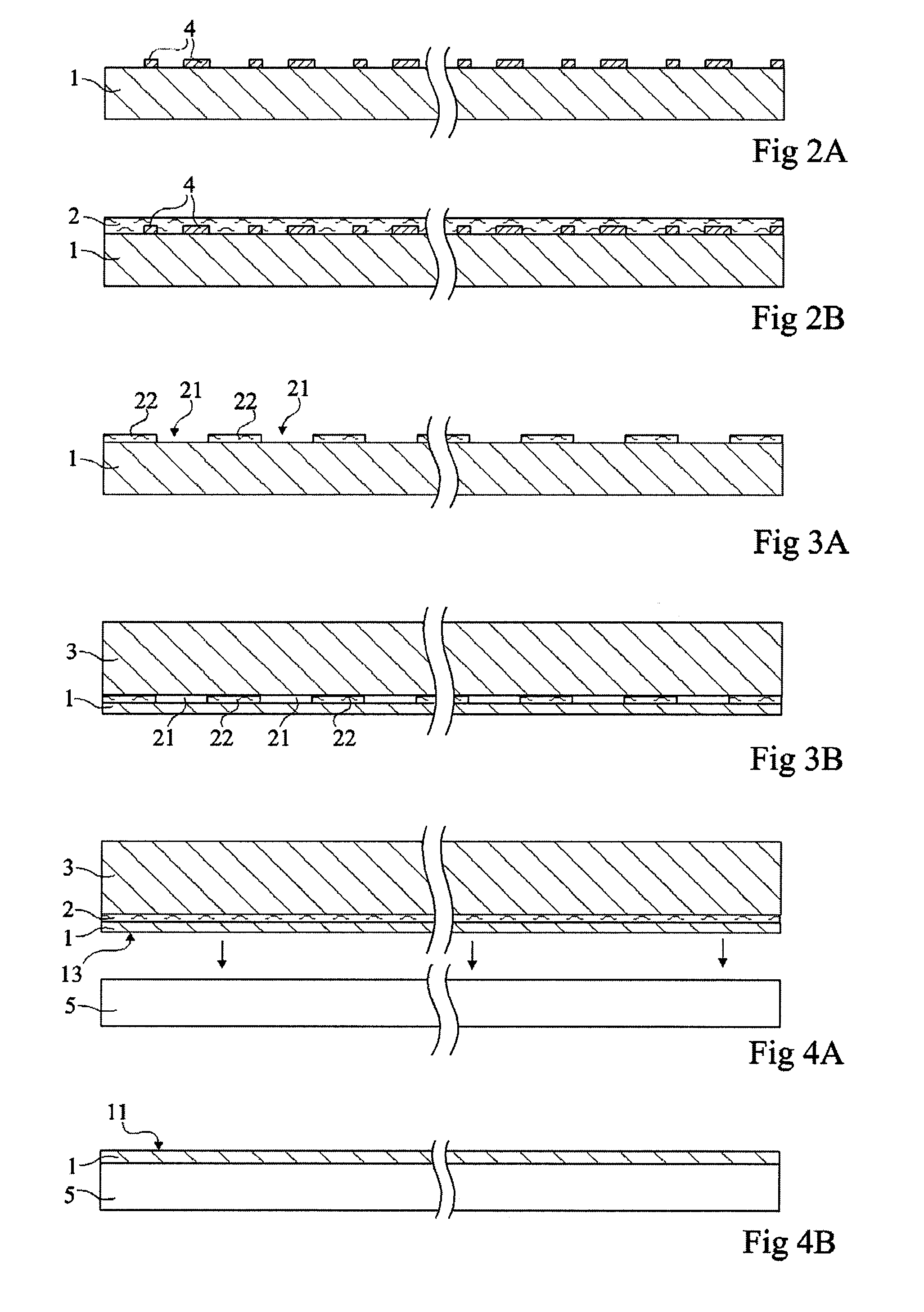
[0048] The same elements have been designated the same reference numerals in the different drawings which have been drawn out of scale. For clarity, only those steps and elements which are necessary to the understanding of the present invention have been shown in the drawings and will be described hereafter. In particular, the steps of integrated circuit manufacturing on the semiconductor wafer have not been detailed, the present invention being compatible with any conventional electronic circuit manufacturing method. Similarly, the actual thinning of a semiconductor wafer supported by a substrate according to the present invention has not been detailed, the present invention being here again compatible with all conventional thinning techniques.

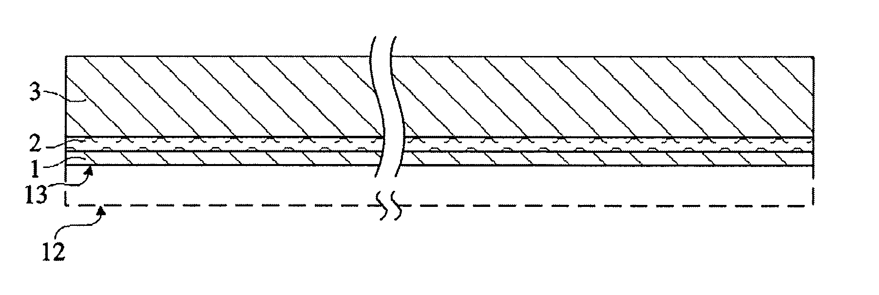
[0049] According to a preferred embodiment of the present invention, a first semiconductor wafer to be thinned down from a first surface is placed by its first surface on a substrate formed of a second wafer, preferably of same nature, with ...


PUM

PropertyMeasurementUnit
thicknessaaaaaaaaaa
thicknessaaaaaaaaaa
thicknessaaaaaaaaaa

Abstract

A method for processing a first semiconductor wafer having a first surface and a second surface, by placing, on the second surface of the first wafer, a second wafer with an interposed resist layer, and thinning down the first surface of the first semiconductor wafer.

Description

BACKGROUND OF THE INVENTION [0001] 1. Technical Field [0002] The present invention relates to the field of microelectronics and, more specifically, to the thinning of a wafer made of a semiconductor material in which electronic circuits have been manufactured or which is intended to be used to manufacture such circuits. [0003] 2. Description of the Related Art [0004] Thinning down integrated circuits or wafers of a semiconductor material supporting such circuits is a constant need of the microelectronics industry. Such a thinning down to thicknesses of a few tens of micrometers or even a few micrometers provides many possibilities in terms of applications for the electronic circuits thus formed. Thin integrated circuit chips are likely to be used in many electronic applications, be it independently or for assembly to other chips or substrates. [0005] Among such applications, the integration of electromagnetic transponders to form very thin electronic tags likely to be supported by b...

Claims


Application Information

Patent Timeline
Patent Type & Authority Applications(United States)
IPC IPC(8): H01L21/461H01L21/46
CPCH01L21/6835H01L21/78H01L25/50H01L31/18H01L2221/6834H01L2221/68363H01L2924/0002H01L2924/00
Inventor HERNANDEZ, CAROLINE
Owner STMICROELECTRONICS SRL
Why Eureka
Try Eureka