Undoped gate poly integration for improved gate patterning and cobalt silicide extendibility

a technology of cobalt silicide and polyintegration, which is applied in the direction of semiconductor/solid-state device manufacturing, basic electric elements, electric apparatus, etc., can solve the problems of irregular gate profile, deviating substantially from the ideal vertical sidewall, and difficult to control the vertical profile of polysilicon gates

Inactive Publication Date: 2007-09-20
NORTH STAR INNOVATIONS
View PDF4 Cites 82 Cited by
  • Summary
  • Abstract
  • Description
  • Claims
  • Application Information

AI Technical Summary

Problems solved by technology

Each type of processing may contribute separately to the etching of the polysilicon gate, making it difficult to control the vertical profiles of polysilicon gates.
These etch and clean steps—in conjunction with doping, nitrogen implant (for PMOS gates) and implant damage—result in an irregular...

Method used


Image

  • Undoped gate poly integration for improved gate patterning and cobalt silicide extendibility
  • Undoped gate poly integration for improved gate patterning and cobalt silicide extendibility
  • Undoped gate poly integration for improved gate patterning and cobalt silicide extendibility

Examples


Embodiment Construction

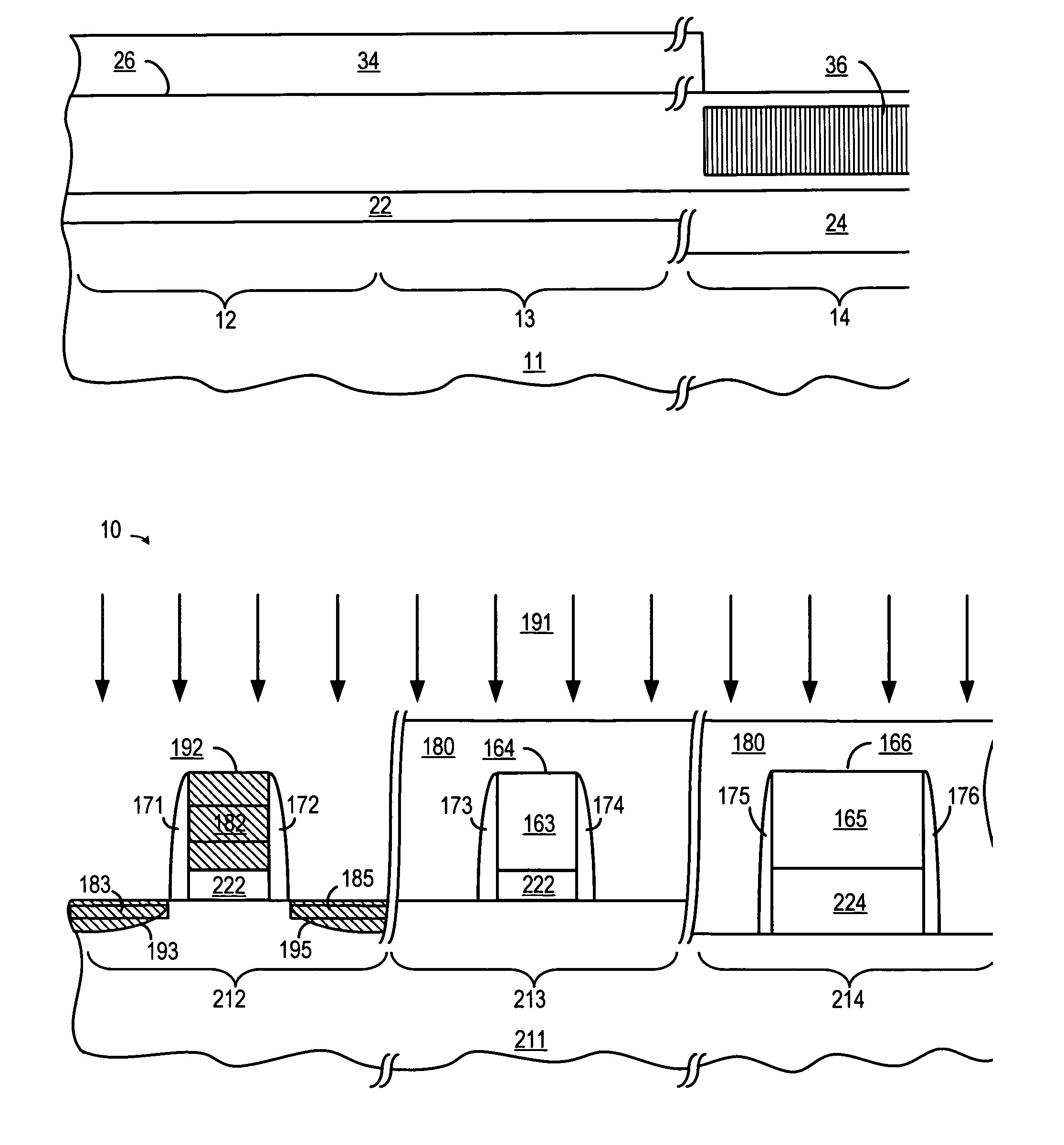
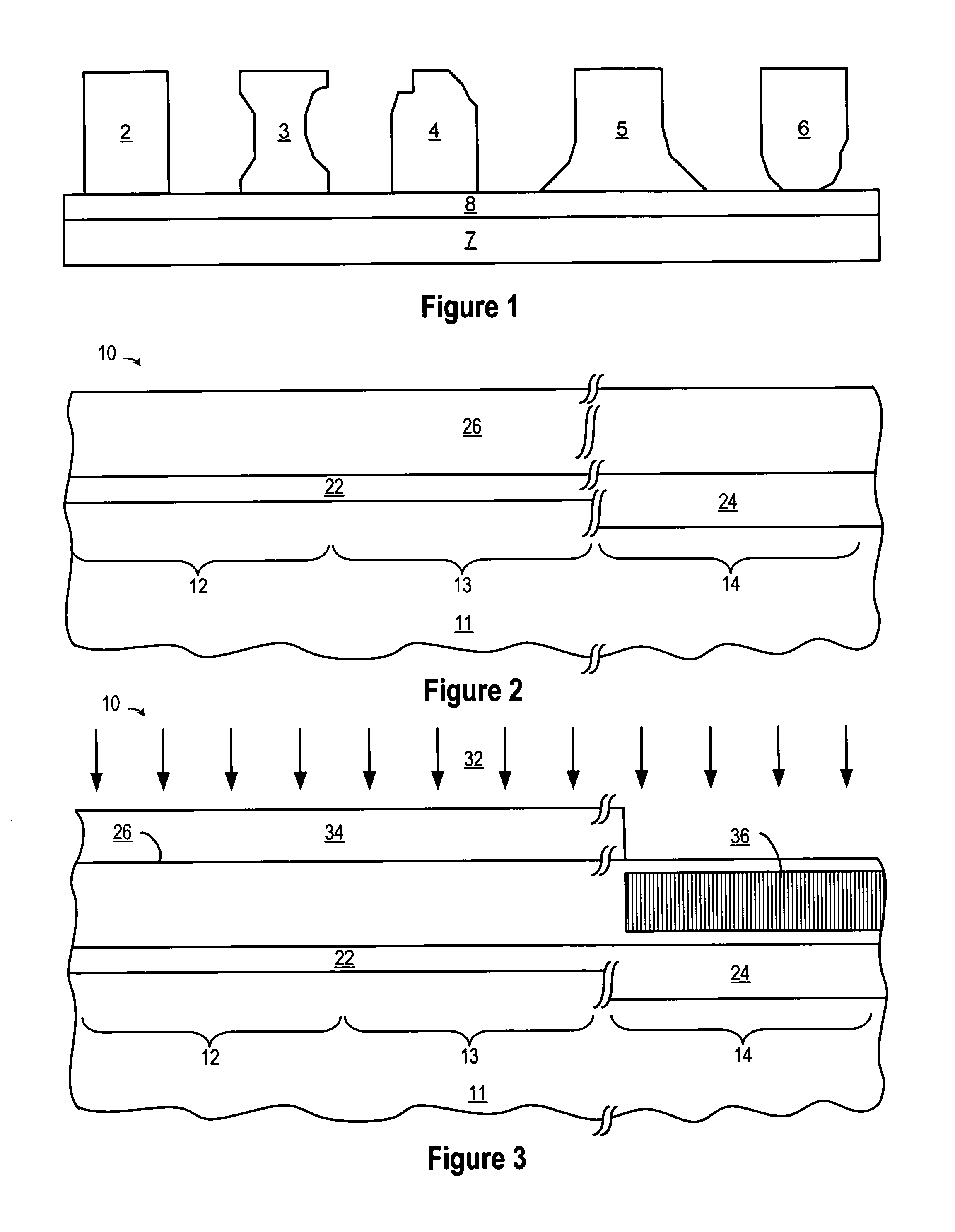
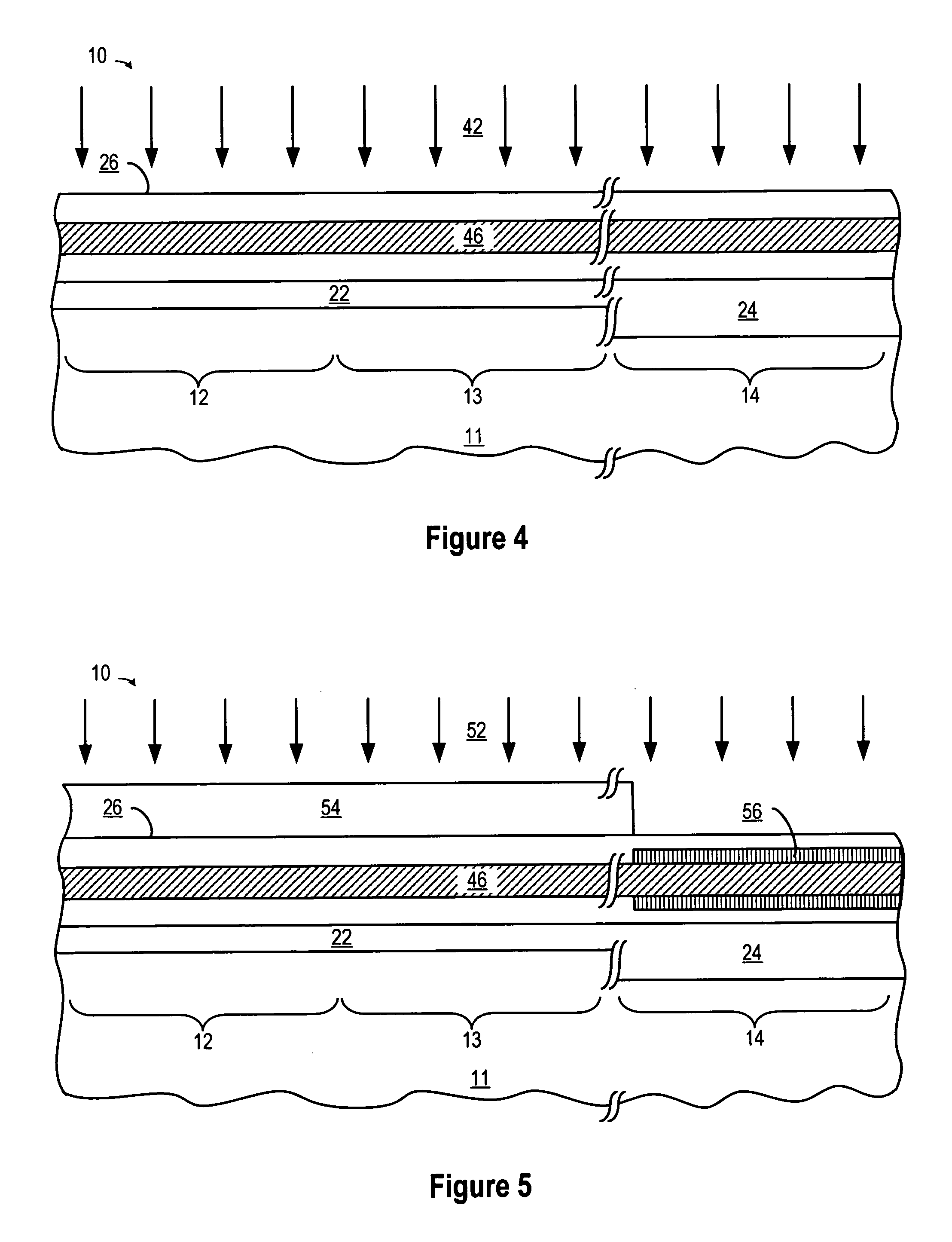
[0022] A method and apparatus are described for fabricating a silicon-based device feature, such as a transistor gate or a fin of a FinFET device, by etching an undoped polysilicon layer to form etched gate electrode structures having improved, more vertical sidewall profiles, and then subsequently doping the etched gate electrode structures during implantation of the source / drain regions. In this embodiment where undoped poly is etched, any differences between the gate etch profiles for N-doped Poly gates and P-doped Poly gates is eliminated. In another embodiment, an implant species (e.g., nitrogen) may be implanted in all or part of the undoped polysilicon layer prior to gate etch which is tuned to reduce or eliminate hour-glassing associated with nitrogen-doped polysilicon profiles. In yet another embodiment, the implant species may be implanted after forming sidewall spacers on etched gate electrode structures from undoped polysilicon, in which case the subsequent doping of t...


PUM


Abstract

A semiconductor process and apparatus uses a predetermined sequence of patterning and etching steps to etch an intrinsic polysilicon layer (26) formed over a substrate (11), thereby forming etched gates (62, 64) having vertical sidewall profiles (61, 63). While a blanket nitrogen implant (46) of the intrinsic polysilicon layer (26) may occur prior to gate etch, more idealized vertical gate sidewall profiles (61, 63) are obtained by fully doping the gates (80, 100) during the source/drain implantation steps (71, 77, 91, 97) and after the gate etch.

Description

BACKGROUND OF THE INVENTION [0001] 1. Field of the Invention [0002] The present invention is directed in general to the field of semiconductor devices. In one aspect, the present invention relates to controlling the profile of semiconductor features in semiconductor devices. [0003] 2. Description of the Related Art [0004] As semiconductor device sizes are scaled down, the requirements for device design and fabrication continue to be tightened in order to fit more circuitry on smaller chips. As device sizes shrink, increasingly complex etch processes are used to define semiconductor device features, such as polysilicon gates. For example, a typical gate patterning process may use several steps after the doped polysilicon layer is formed and the photoresist (“PR”) is patterned, including a PR trim step (to shrink the size of the features being transferred), a hard mask etch step (which uses the PR as a mask), an ARC etch step (which uses the hard mask as a mask), a preliminary cleanin...

Claims


Application Information

Patent Timeline
IPC IPC(8): H01L21/04
CPCH01L21/823418H01L21/823462H01L21/823456H01L21/82345
Inventor SHROFF, MEHUL D.GRUDOWSKI, PAUL A.HALL, MARK D.STEPHENS, TAB A.
Owner NORTH STAR INNOVATIONS
Why Eureka
Try Eureka