Circuit-pattern-data correction method and semiconductor-device manufacturing method

a technology of circuit-pattern data and manufacturing method, which is applied in the direction of photomechanical treatment originals, instruments, photomechanical equipment, etc., can solve the problems of broken lines, difficult to correct factors, etc., and achieve the effect of preventing excessive correction

Inactive Publication Date: 2007-09-20
FUJITSU SEMICON LTD
View PDF12 Cites 11 Cited by
  • Summary
  • Abstract
  • Description
  • Claims
  • Application Information

AI Technical Summary

Benefits of technology

[0016]In view of the foregoing, it is an object of the present invention to provide a circuit-pattern-data correction method capable of preventing excessive correction made by the model-based OPC and caused by a step (difference in level) located close to a circuit pattern corner, the step being generated when the rule-based OPC is applied.

Problems solved by technology

Since the model-based OPC is based on optical-intensity simulation, it is difficult to correct factors, such as the influence of etching, caused by processes other than lithography.
If a step produced when the rule-based OPC is applied is located in a vicinity of a circuit pattern corner, overcorrection is made by the model-based OPC, which is the next step, to cause a broken line and other problems.

Method used


Image

  • Circuit-pattern-data correction method and semiconductor-device manufacturing method
  • Circuit-pattern-data correction method and semiconductor-device manufacturing method
  • Circuit-pattern-data correction method and semiconductor-device manufacturing method

Examples


Embodiment Construction

[0039]Embodiments of the present invention will be described below by referring to the drawings.

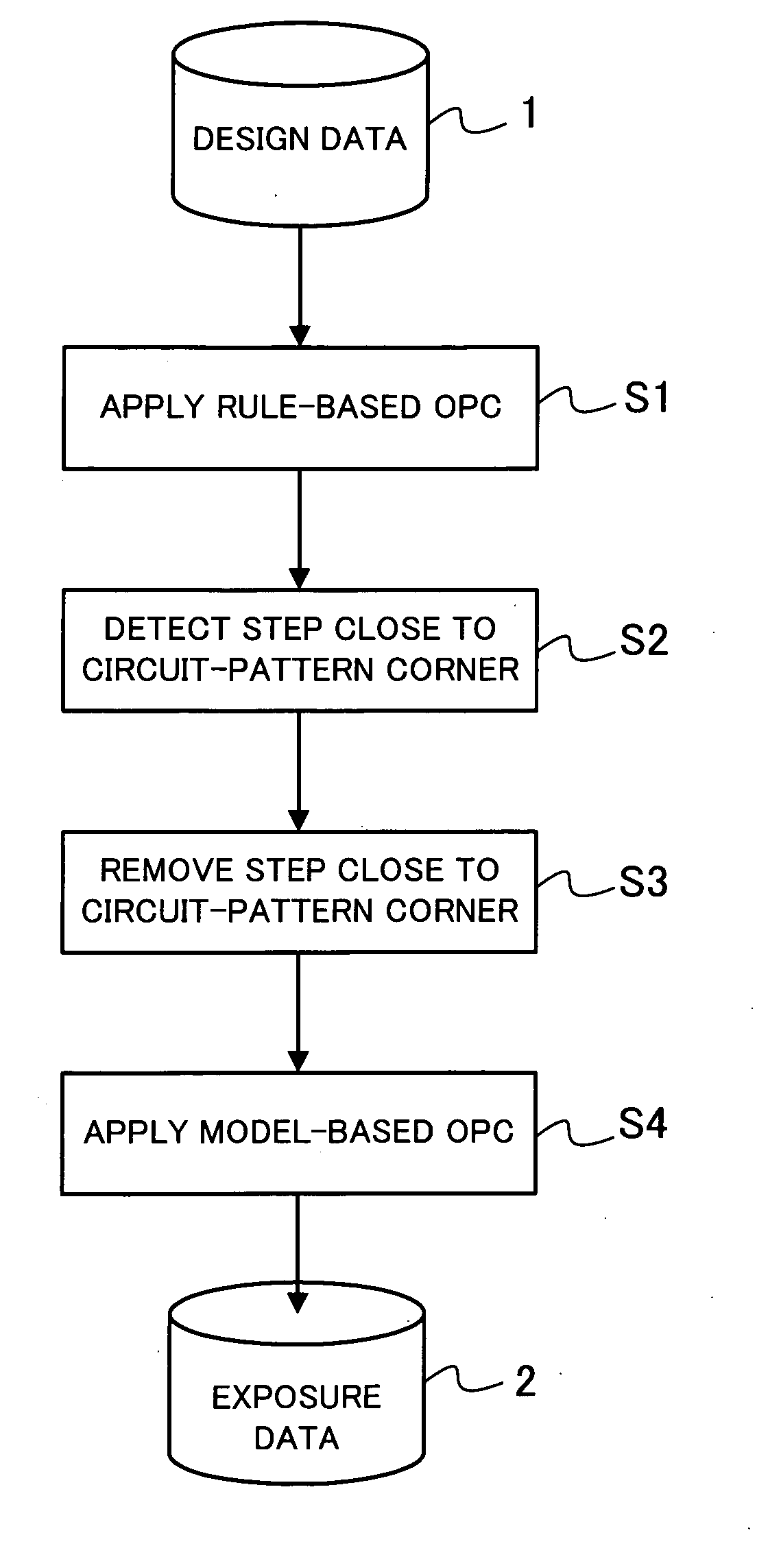
[0040]FIG. 1 is a flowchart showing an outline of a circuit-pattern-data correction method according to an embodiment of the present invention.

[0041]In the circuit-pattern-data correction method according to the present embodiment, proximity-effect correction based on rule-based OPC is applied in step S1 to design data 1 of a photomask such as a reticle or of a circuit pattern formed on a wafer.

[0042]The rule-based OPC corrects the input design data 1 by using a correction table. The correction table specifies the amount of correction according to the width of a circuit pattern and the distance to an adjacent circuit pattern. For example, when the distance from a target circuit pattern to an adjacent circuit pattern is a predetermined distance or more, the width of the target circuit pattern is made thicker, or when an adjacent circuit pattern is located close, the width of the target cir...


PUM

PropertyMeasurementUnit
widthaaaaaaaaaa
widthaaaaaaaaaa
lengthaaaaaaaaaa

Abstract

Circuit-pattern-data correction method and semiconductor-device manufacturing method which prevent excessive correction from being made when model-based proximity-effect correction (OPC) is applied to a corrected circuit pattern, the excessive correction being caused by a step (difference in level) close to a circuit-pattern corner in the corrected circuit pattern, and the step being produced when rule-base OPC is applied. The rule-based OPC is applied to input design data in step S1; a step close to a circuit-pattern corner, produced by the rule-based OPC is detected in step S2; the step is removed in step S3; and the model-based OPC is applied and exposure data is generated in step S4.

Description

CROSS-REFERENCE TO RELATED APPLICATIONS[0001]This application is based upon and claims the benefits of priority from the prior Japanese Patent Application No. 2006-076642, filed on Mar. 20, 2006, the entire contents of which are incorporated herein by reference.BACKGROUND OF THE INVENTION[0002]1. Field of the Invention[0003]The present invention relates to circuit-pattern-data correction methods and semiconductor-device manufacturing methods, and particularly to a circuit-pattern-data correction method and a semiconductor-device manufacturing method which reduce the influence of a proximity effect, produced when a circuit pattern is formed on a wafer according to design data for a semiconductor device.[0004]2. Description of the Related Art[0005]As semiconductor devices have been using finer patterns due to higher integration these days, the influence of a proximity effect appears greatly in an exposure process, disabling semiconductor devices to be manufactured according to the des...

Claims


Application Information

Patent Timeline
Patent Type & Authority Applications(United States)
IPC IPC(8): G06F17/50G03F1/36G03F1/68H01L21/027
CPCG03F1/36G03F1/144
Inventor SAGISAKA, ATSUSHICHIJIMATSU, TATSUO
Owner FUJITSU SEMICON LTD
Why Eureka
Try Eureka