Light-emitting element, light-emitting device, and electronic device

a technology of light-emitting devices and elements, applied in the direction of discharge tube luminescnet screens, organic chemistry, natural mineral layered products, etc., can solve the problems of short life of elements, inability to obtain favorable light-emitting efficiency, and problems such as the problem of element life, to achieve the effect of high luminous efficiency, long life and high luminous efficiency

Active Publication Date: 2007-09-27
SEMICON ENERGY LAB CO LTD
View PDF77 Cites 98 Cited by
  • Summary
  • Abstract
  • Description
  • Claims
  • Application Information

AI Technical Summary

Benefits of technology

[0028]By implementation of the present invention, a light-emitting element with high luminous efficiency can be provided. In particular, a light-emitting element with high luminous efficiency and long life can be provided.
[0029]Further, by manufacture of a light-emitting device using the light-emitting element described above, a light-emitting device with low power consumption and long life can be provided. Further, by application of such a light-emitting device to an electronic device, an electronic device with low power consumption and long life can be provided.

Problems solved by technology

According to the report in Non Patent Document 1 described above, the half-life of luminance is about 170 hours when the initial luminance is set to be 500 cd / m2 in constant current driving, and so, there is a problem on the life of the element.
In Non Patent Document 1, it is said that the element has short life since stability of BCP is insufficient, though the BCP is used as a hole blocking layer.
However, if BCP is removed from an element structure in Non Patent Document 1, light emission with favorable efficiency cannot be obtained.
However, contrary to Non Patent Document 1, it is necessary to select a material of a hole transporting layer in a limited way.

Method used


Image

  • Light-emitting element, light-emitting device, and electronic device
  • Light-emitting element, light-emitting device, and electronic device
  • Light-emitting element, light-emitting device, and electronic device

Examples


embodiment mode 1

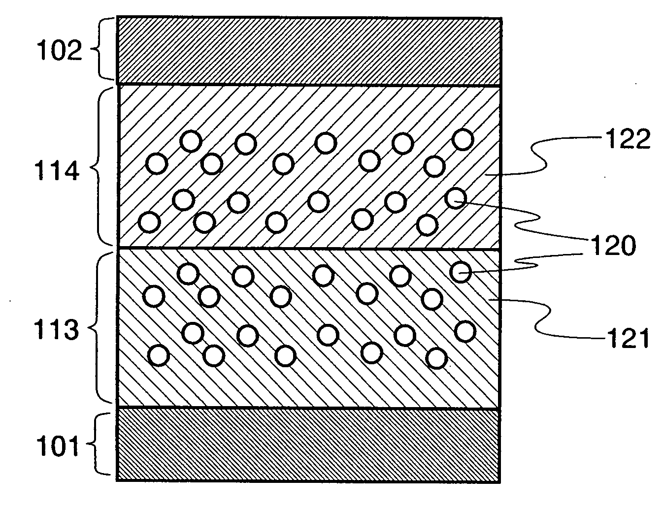
[0049]In Embodiment Mode 1, a most basic structure of a light-emitting element of the present invention will be explained with reference to FIG. 1.

[0050]FIG. 1 shows a light-emitting element of the present invention having a first light-emitting layer 113 and a second light-emitting layer 114 provided to be in contact with each other between a first electrode 101 and a second electrode 102, where the first light-emitting layer 113 includes a hole transporting host material 121 and a phosphorescent compound 120, and the second light-emitting layer 114 includes an electron transporting host material 122 and the phosphorescent compound 120. That is, the phosphorescent compound added to the first light-emitting layer 113 and the phosphorescent compound added to the second light-emitting layer 114 are the same compound. The phosphorescent compound is dispersed in the first light-emitting layer 113 and the second light-emitting layer 114 as a guest material.

[0051]With such a structure, in...

embodiment mode 2

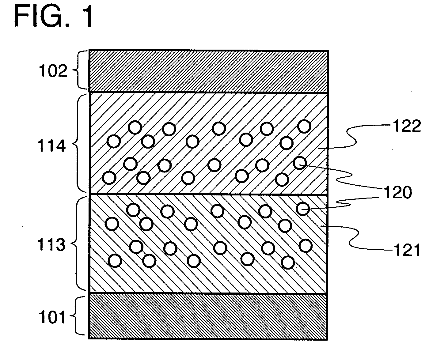
[0059]In Embodiment Mode 2, the structure of the light-emitting element of the present invention will be explained in more detail. FIG. 2 shows an element structure thereof.

[0060]FIG. 2 shows a light-emitting element of the present invention having a first light-emitting layer 213 and a second light-emitting layer 214 provided to be in contact with each other between a first electrode 201 serving as an anode and a second electrode 202 serving as a cathode, where the first light-emitting layer 213 includes a hole transporting host material 221 and a phosphorescent compound 220, and the second light-emitting layer 214 includes an electron transporting host material 222 and the phosphorescent compound 220. That is, the phosphorescent compound added to the first light-emitting layer 213 and the phosphorescent compound added to the second light-emitting layer 214 are the same. The phosphorescent compound is dispersed in the first light-emitting layer and the second light-emitting layer a...

embodiment mode 3

[0082]Embodiment Mode 3 explains a mode of a light-emitting device including the light-emitting element of the present invention with reference to FIGS. 4A to 4C. FIGS. 4A to 4C show cross-sectional views of the light-emitting device.

[0083]In FIGS. 4A to 4C, a portion surrounded by dotted lines of a rectangular shape is a transistor 11 which is provided to drive a light-emitting element 12 of the present invention. The light-emitting element 12 is a light-emitting element of the present invention in which a layer 15 including a light-emitting layer is formed between a first electrode 13 and a second electrode 14. Specifically, the light-emitting element 12 has the structure as shown in Embodiment Modes 1 and 2. A drain region of the transistor 11 is electrically connected to the first electrode 13 by a wiring 17 penetrating a first interlayer insulating film 16 (16a, 16b, and 16c). The light-emitting element 12 is separated from other adjacently-provided light-emitting elements by a...


PUM

PropertyMeasurementUnit
emission wavelengthaaaaaaaaaa
energy gapaaaaaaaaaa
internal quantum efficiencyaaaaaaaaaa

Abstract

It is an object to provide an element structure which is suitable for a light-emitting element using a phosphorescent compound. It is another object to provide a light-emitting element with high luminous efficiency by using the element structure. In particular, it is another object to provide a light-emitting element with high luminous efficiency and long life. A light-emitting element is manufactured, which includes a first light-emitting layer and a second light-emitting layer provided to be in contact with each other between a first electrode and a second electrode, where the first light-emitting layer includes a hole transporting host material and a phosphorescent compound, and the second light-emitting layer includes an electron transporting host material and the phosphorescent compound.

Description

BACKGROUND OF THE INVENTION[0001]1. Field of the Invention[0002]The present invention relates to a light-emitting element using a phosphorescent compound. Further, the present invention relates to a light-emitting device using the light-emitting element. Furthermore, the present invention relates to an electronic device using the light-emitting device.[0003]2. Description of the Related Art[0004]In recent years, a light-emitting element using a light-emitting organic compound or inorganic compound as a light-emitting substance has been actively developed. In particular, a light-emitting element called an EL element has a simple structure in which a light-emitting layer containing a light-emitting substance is provided between electrodes. Therefore, the light-emitting element has attracted attention as a next-generation flat panel display element because of its characteristics such as a thin shape, lightweight, high response speed, and direct current driving at low voltage. In additi...

Claims


Application Information

Patent Timeline
Patent Type & Authority Applications(United States)
IPC IPC(8): H01L51/54
CPCH01L51/5016H10K50/11H10K2101/10C07D413/10C09K11/06H10K85/649H10K50/13H10K50/165H10K50/16H10K50/15H10K50/81H10K50/82H10K50/121H10K71/831
Inventor OHSAWA, NOBUHARUSEO, SATOSHIMURATA, HIROKO
Owner SEMICON ENERGY LAB CO LTD
Why Eureka
Try Eureka