
Semiconductor memory device

Inactive Publication Date: 2007-09-27
KK TOSHIBA
View PDF10 Cites 2 Cited by
  • Summary
  • Abstract
  • Description
  • Claims
  • Application Information

AI Technical Summary

Benefits of technology

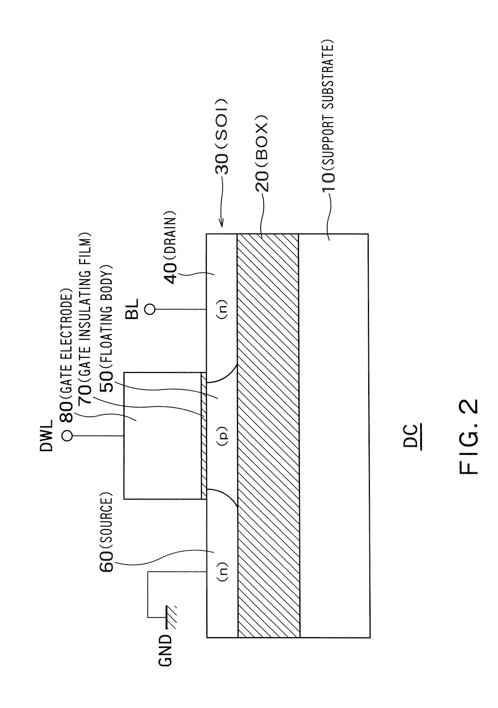
[0008]A semiconductor memory device according to an embodiment of the present invention comprises a first memory cell including a floating body in an electrically floating state and storing data according to the number of majority carriers in the floating body; a word line connected to a gate of the first memory cell; a first bit line connected to the first memory cell to transmit the data stored in the first memory cell; a second bit line transmitting reference data used to detect the data stored in the first memory cell; a first sense node and a second sense node transmitting the data stored in the first memory cell and the reference data, respectively; a first short-circuiting switch provided between the first sense node and the second sense node; and a first flip-flop applying a load current to the first memory cell during a data read operation and detecting a potential difference generated between the first sense node and th

Problems solved by technology

However, since both the current load circuit and the CMOS latch circuit are provided, the circuit scale of the sense amplifier is disadvantageously large.
Furthermore, such a sense amplifier needs to wait until a potential difference between the pair of sense nodes exceeds the irregularity in the threshold voltages among the transistors.
Therefore, the sense amplifier has a disadvantage the data detection speed is decreased.
This disadvantageously increases current consumption of the conventional sense amplifier.

Method used


Image

  • Semiconductor memory device
  • Semiconductor memory device
  • Semiconductor memory device

Examples


first embodiment

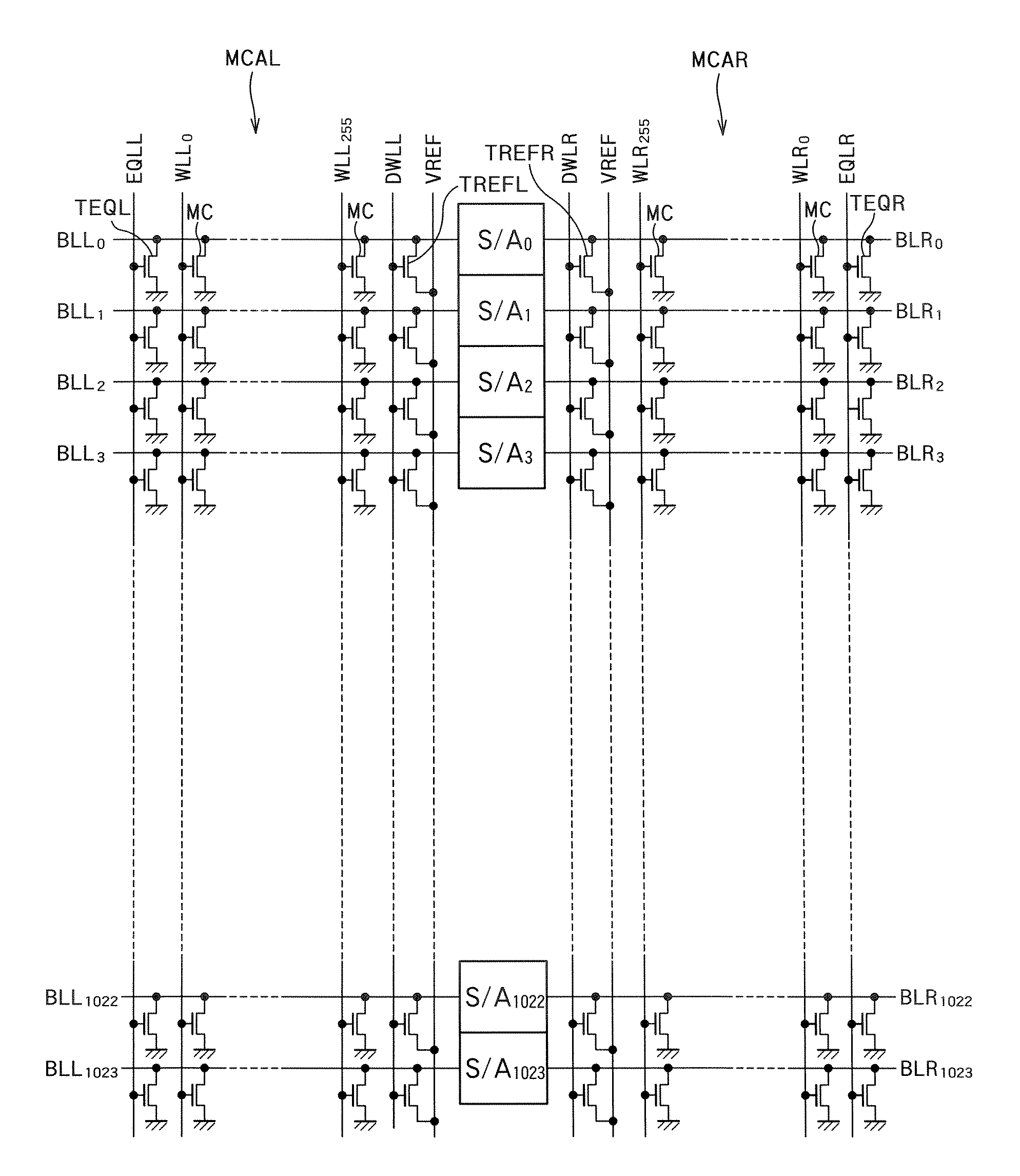
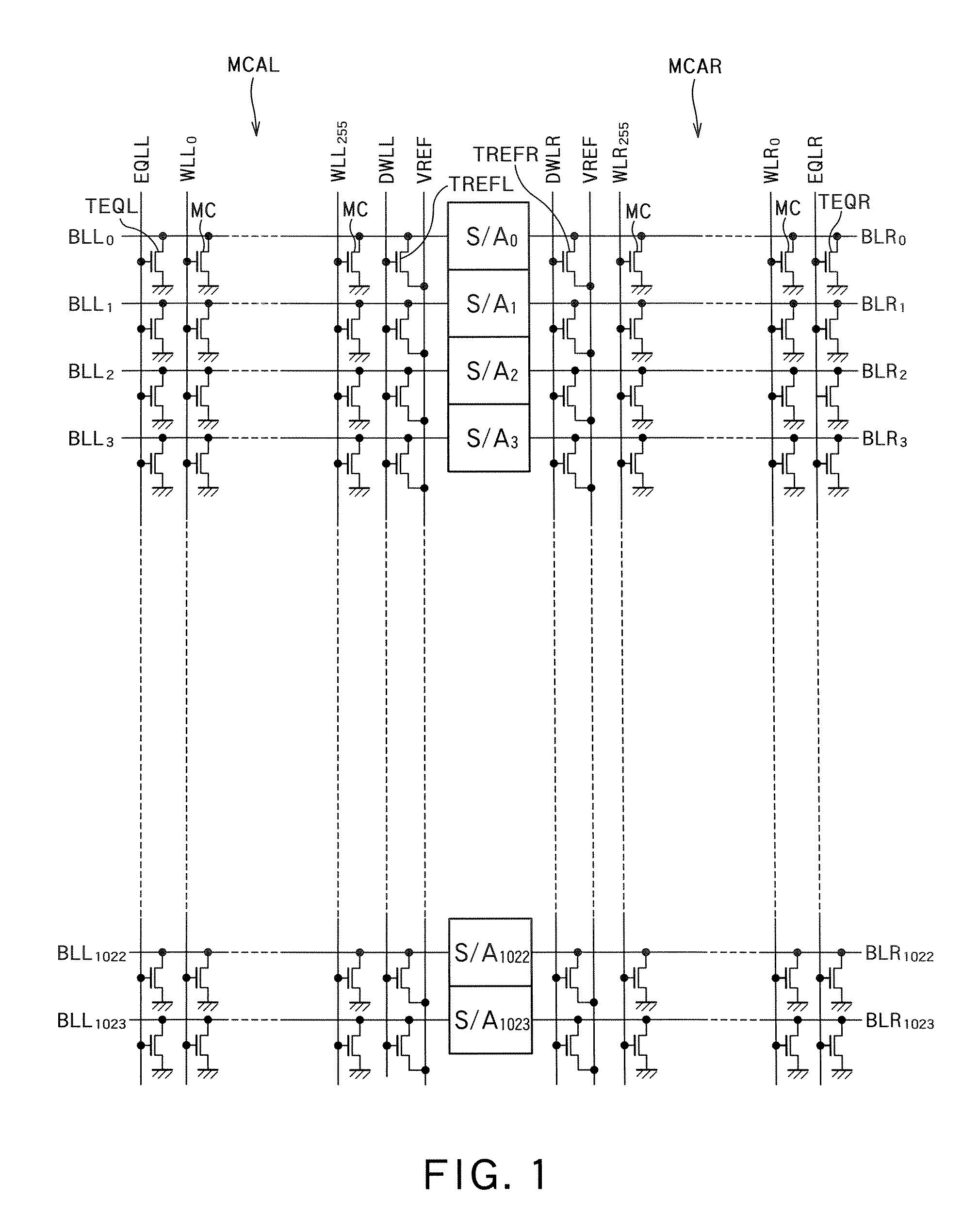
[0041]FIG. 1 is a circuit diagram of the configuration of an FBC memory device according to a first embodiment of the present invention. The FBC memory device includes memory cells MC, sense amplifiers S / Ai (where i is an integer) (hereinafter, also “S / A”), word lines WLLi and WLRi (hereinafter, also “WL”), bit lines BLLi and BLRi (hereinafter, also “BL”), equalizing lines EQLL and EQLR (hereinafter, also “EQL”), equalizing transistors TEQL and TEQR (hereinafter, also “TEQ”), reference potential lines VREF, reference transistors TREFL and TREFR (hereinafter, also “TREF”), and dummy word lines DWLL and DWLR (hereinafter, also “DWL”). It is to be noted that “reference potential” refers to a voltage with which data “1” or “0” is compared when the data “1” or “0” is detected.

[0042]The memory cells MC are arranged in a matrix and memory cell arrays MCAL and MCAR (hereinafter, also “MCA”) are constituted by the memory cells MC. The word lines WL extend in a row direction and are connected...

second embodiment

[0079]FIG. 8 is a circuit diagram of a sense amplifier S / A according to a second embodiment of the present invention. The sense amplifier S / A according to the second embodiment differs from that according to the first embodiment in that the sense amplifier S / A includes a first flip-flop FF11 constituted by PMOS transistors TP10 and TP11 and a second flip-flop FF12 constituted by PMOS transistors TP12 and TP13 instead of the flip-flops FF1. The other configurations of the sense amplifier S / A according to the second embodiment can be the same as those according to the first embodiment.

[0080]The transistors TP10 and TP11 are connected in series between the sense nodes SNL and SNR. The transistors TP12 and TP13 are connected in series between the sense nodes SNL and SNR. Gates of the transistors TP10 and TP12 are connected in common to the sense node SNR. Gates of the transistors TP11 and TP13 are connected in common to the sense node SNL. Namely, the gates of the transistors TP10 and T...

third embodiment

[0088]FIG. 10 is a circuit diagram of a sense amplifier S / A according to a third embodiment of the present invention. The sense amplifier S / A according to the third embodiment differs from that according to the second embodiment in that the sense amplifier S / A according to the third embodiment includes a PMOS transistor TP30 serving as a first short-circuiting switch and a PMOS transistor TP31 serving as a second short-circuiting switch in place of the PMOS transistor TP3 shown in FIG. 8. The other configurations of the sense amplifier S / A according to the third embodiment can be the same as those according to the second embodiment. The sum of sizes (W / L) of the transistors TP30 and TP31 can be set almost equal to the size (W / L) of the transistor TP3 according to the first and the second embodiments. The size (W / L) of the transistor TP30 needs to be sufficiently large to quickly equalize the paired sense nodes during precharging (before to and after t8). However, the size (W / L) of t...


PUM


Abstract

This disclosure concerns a memory including a memory cell including a floating body in an electrically floating state and storing data according to the number of majority carriers in the floating body; a word line connected to a gate of the memory cell; a first bit line connected to the memory cell to transmit the data; a second bit line transmitting reference data used to detect the data stored in the memory cell; a first sense node and a second sense node transmitting the data stored in the memory cell and the reference data, respectively; a first short-circuiting switch provided between the first sense node and the second sense node; and a first flip-flop applying a load current to the memory cell during a data read operation and amplifying a potential difference generated between the first sense node and the second sense node by turning off the first short-circuiting switch

Description

CROSS-REFERENCE TO RELATED APPLICATION[0001]This application is based upon and claims the benefit of priority from the prior Japanese Patent Applications No. 2006-83189, filed on Mar. 24, 2006, the entire contents of which are incorporated herein by reference.BACKGROUND OF THE INVENTION[0002]1. Field of the Invention[0003]The present invention relates to a semiconductor memory device and relates to, for example, a sense amplifier for an FBC (Floating Body Cell).[0004]2. Related Art[0005]A sense amplifier employed in a conventional FBC-DRAM includes a current load circuit and a CMOS latch circuit connected to a pair of sense nodes. The sense amplifier including both the current load circuit and the CMOS latch circuit can advantageously ensure accurately detecting data, i.e., can be advantageously robust against irregularity in a threshold voltage among transistors that constitute the sense amplifier. However, since both the current load circuit and the CMOS latch circuit are provided...

Claims


Application Information

Patent Timeline
IPC IPC(8): G11C11/34G11C7/00
CPCG11C7/12G11C7/14G11C11/404G11C11/4091G11C2211/4016G11C11/4099G11C2207/002G11C2207/005G11C2207/2281G11C11/4094
Inventor OHSAWA, TAKASHI
Owner KK TOSHIBA
Learn More