Semiconductor device and method of manufacturing the same

a technology of semiconductors and semiconductors, applied in the direction of semiconductor devices, basic electric elements, electrical appliances, etc., can solve the problems of difficult to uniformly form the gate insulating film, and difficult to obtain a desirable threshold voltage vth

Inactive Publication Date: 2007-09-27
LONGITUDE SEMICON S A R L
View PDF7 Cites 28 Cited by
  • Summary
  • Abstract
  • Description
  • Claims
  • Application Information

AI Technical Summary

Benefits of technology

[0019] Another object of the present invention is to provide a semiconductor device in which a lower portion of a trench is processed to a shape of a true circle, while suppressing a residue generated when the trench is formed by etching, and a method of manufacturing the same.

Problems solved by technology

Consequently, it is difficult to obtain a desirable threshold voltage Vth.
However, when the miniaturization is further advanced, it is difficult to obtain a desirable threshold voltage Vth even in the semiconductor device of the embedded type as mentioned above.
Moreover, when the isotropic etching is carried out, a residue (crystal defect) is generated inside the trench, and it becomes difficult to uniformly form the gate insulating film.
However, any of the foregoing conventional examples does not disclose a technique for processing the lower sectional shape of the trench to a shape close to the true circle, while suppressing the residue generated inside the trench.

Method used


Image

  • Semiconductor device and method of manufacturing the same
  • Semiconductor device and method of manufacturing the same
  • Semiconductor device and method of manufacturing the same

Examples


Embodiment Construction

[0040] Hereinafter, a semiconductor device and a method of manufacturing the same according to the present invention will be described in detail with reference to the attached drawings.

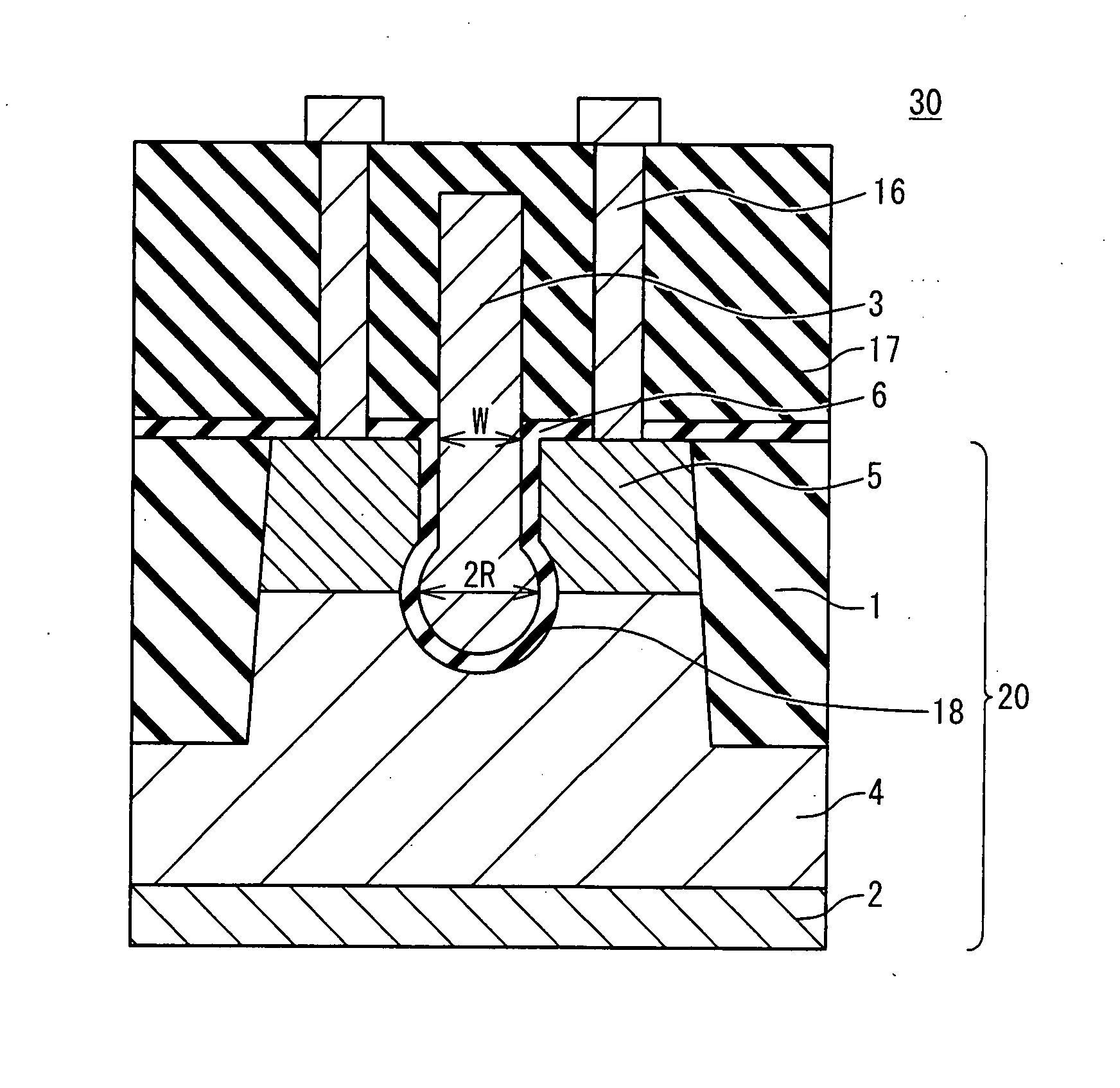
[0041]FIG. 6 is a cross sectional view showing the sectional structure of a semiconductor device 30 according to an embodiment of the present invention. In this embodiment, an n-type channel MOS transistor is exemplified and described as the semiconductor device 30. The semiconductor device 30 has a semiconductor substrate 20, a gate insulating film 6, a gate electrode 3, a silicon oxide layer 17 and electrodes 16. A p-type well layer 2, a channel dope layer 4, n-type diffusion layers 5, a trench 18 and a pair of device separation sections 1 are formed in the semiconductor substrate 20. For example, in a semiconductor memory device, the gate electrode 3 extends in a row direction as a word line (not shown). One of the diffusion layers 5 is connected with a bit line (not shown) extending in a column d...


PUM


Abstract

In a method of manufacturing a semiconductor device, a trench is formed to have an upper quadrangular section and a lower circular section which is formed through a hydrogen annealing process, to extend in a depth direction of a semiconductor substrate. An insulating film is formed on a surface of the trench and a surface of the semiconductor substrate. A conductive film is formed to fill the trench whose surface is covered with the an insulating film. Source / drain regions are formed on both sides of the trench.

Description

BACKGROUND OF THE INVENTION [0001] 1. Field of the Invention [0002] The present invention relates to a semiconductor device and a method of manufacturing the same. [0003] 2. Description of the Related Art [0004] A semiconductor device is known in which an n-type diffusion layers, a gate insulating film and a gate electrode are formed in a semiconductor substrate. FIG. 1 is a cross section view showing the structure of a conventional semiconductor device. In the semiconductor device, a transistor structure is formed between trench type device isolation sections of a pair. Specifically, the n-type diffusion layers for a source region and a drain region are formed in the surface of the semiconductor substrate having a p-type well layer and a channel dope layer. The gate insulating film is formed on the substrate surface. A gate electrode 3 is formed through the gate insulating film on the substrate surface between the source region and the drain region. Also, electrodes are formed on t...

Claims


Application Information

Patent Timeline
Patent Type & Authority Applications(United States)
IPC IPC(8): H01L21/336
CPCH01L21/324H01L29/66621H01L29/4236H01L21/3247
Inventor FUJIMOTO, HIROYUKIUEDA, YASUHIKOAISO, FUMIKIKOGA, YUKI
Owner LONGITUDE SEMICON S A R L
Why Eureka
Try Eureka