Reducing electromagnetic interferences

a technology of electromagnetic interference and electronic devices, applied in the direction of transmission, transmission monitoring, electrical apparatus, etc., can solve the problems of spurious emissions, radio systems are becoming more and more sensitive to spurious emissions, and components of the same device may be sensitive to electromagnetic interference, etc., to achieve the effect of reducing electromagnetic interference in selected frequency bands, simple and flexibl

Inactive Publication Date: 2007-09-27
NOKIA CORP
View PDF9 Cites 22 Cited by
  • Summary
  • Abstract
  • Description
  • Claims
  • Application Information

AI Technical Summary

Benefits of technology

[0023] It is an advantage of the invention that it provides a simple and flexible possibility of reducing electromagnetic interferences in selected frequency bands. EMI shieldings are not required, and neither frequency nor phase modulations have to be taken into account in the operation of the components causing the electromagnetic interferences.
[0024] The invention is of a particular advantage for the case that a plurality of first components may be disturbed by one or more second components. In this case, the operating frequency of the active second components may be adjusted anew with each change of the activity status of any of the first components.
[0025] The operating frequency of a component may cause EMI at the operating frequency itself and at its harmonics. In one embodiment of the invention, the operating frequency of an active second component may thus be adjusted specifically such that neither the adjusted operating frequency nor one of its harmonics lie within the at least one known frequency range in which an active first component is adapted to operate.
[0026] The at least one first component can comprise any component that may be sensitive to electromagnetic interferences caused by another component. This is usually the case with radio system components. The at least one first component may thus comprise for instance a Bluetooth™ component, a mobile communication system component—like a GSM or a WCDMA system component—, a WLAN component and / or a satellite based positioning system component—like a GPS, a GLONASS or a Galileo component—, etc.
[0027] The at least one second component can comprise any component that runs the risk of disturbing other components by electromagnetic interferences. They may be for instance non-radio system components using a clock signal for synchronizing their operating frequency. Such a clock signal may be generated within the respective second component or be provided by an external clock generator to the respective second component. The at least one second component may comprise for example a display and / or a camera module, etc.
[0028] In a simple approach, the adjustment depends only on the activity status of at least one first component. For example, a phone may be programmed to change automatically its currently used clock frequencies, when those clock frequencies are known to potentially disturb some other component.

Problems solved by technology

Some of these components may be a source of electromagnetic interferences (EMI), while other components of the same device may be sensitive to electromagnetic interferences.
As an unintentional side effect, the clock oscillator generates radio frequency signals, called spurious emissions, in particular at the operating frequency and its harmonics.
Such radio systems are becoming more and more sensitive to spurious emissions.
In general, the routes can be very complex and any long conducting wire in a printed wiring board (PWB) can act as an antenna.
This process is time-consuming and can typically only decrease the severity of the problem, but not resolve it completely.
With an increasing number of components, it might be particularly difficult and time consuming to find an allowed frequency band for EMI generating components.
Such a search may require physical changes of the mechanics or driving electronics, and the possible use cases could even be limited.
Such a shielding 20, 21, however, increases the costs of the manufacturing process.
A phase modulation of a clock signal, however, might render the use of the clock signal more complex.

Method used


Image

  • Reducing electromagnetic interferences
  • Reducing electromagnetic interferences
  • Reducing electromagnetic interferences

Examples


Embodiment Construction

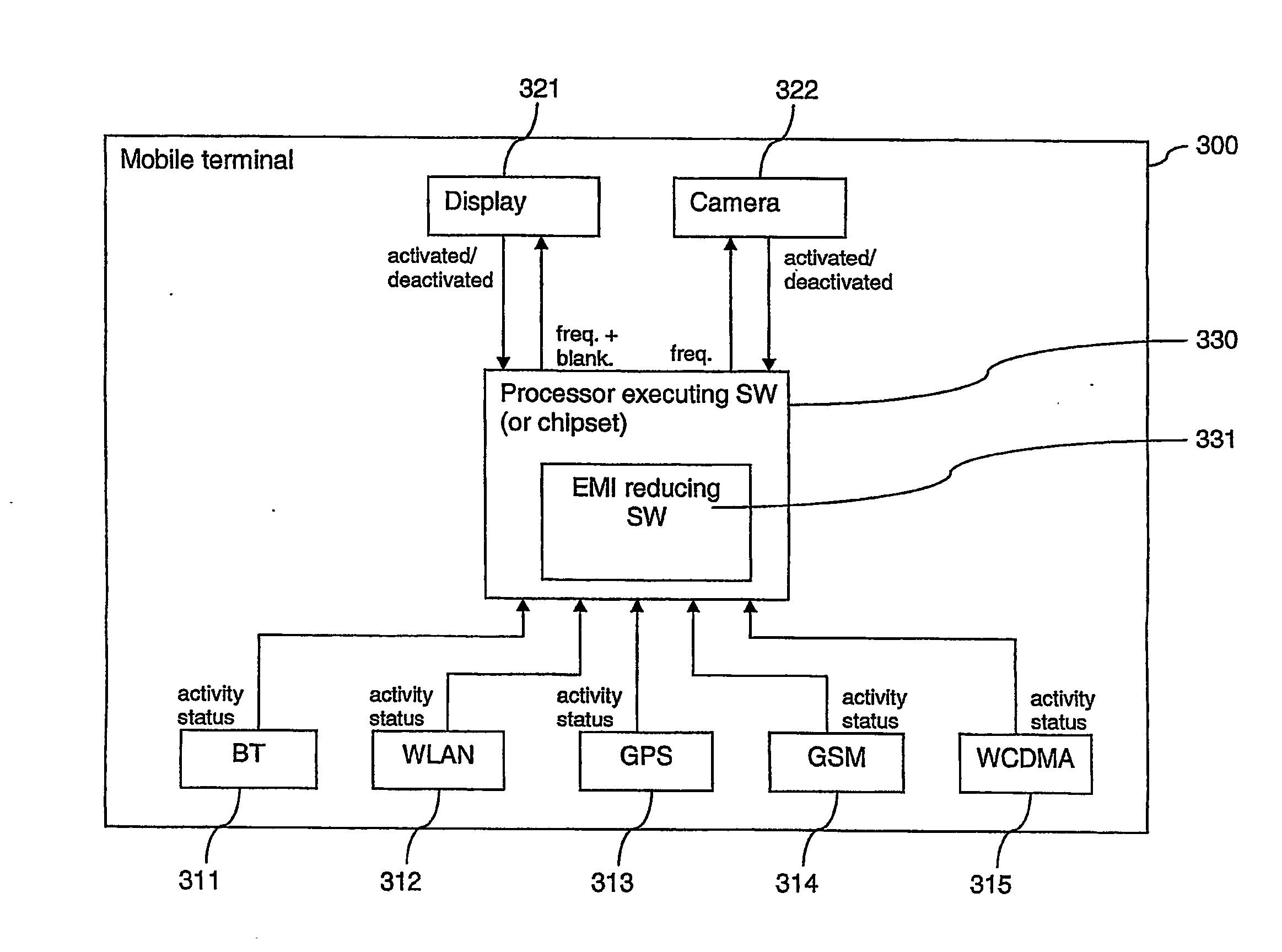
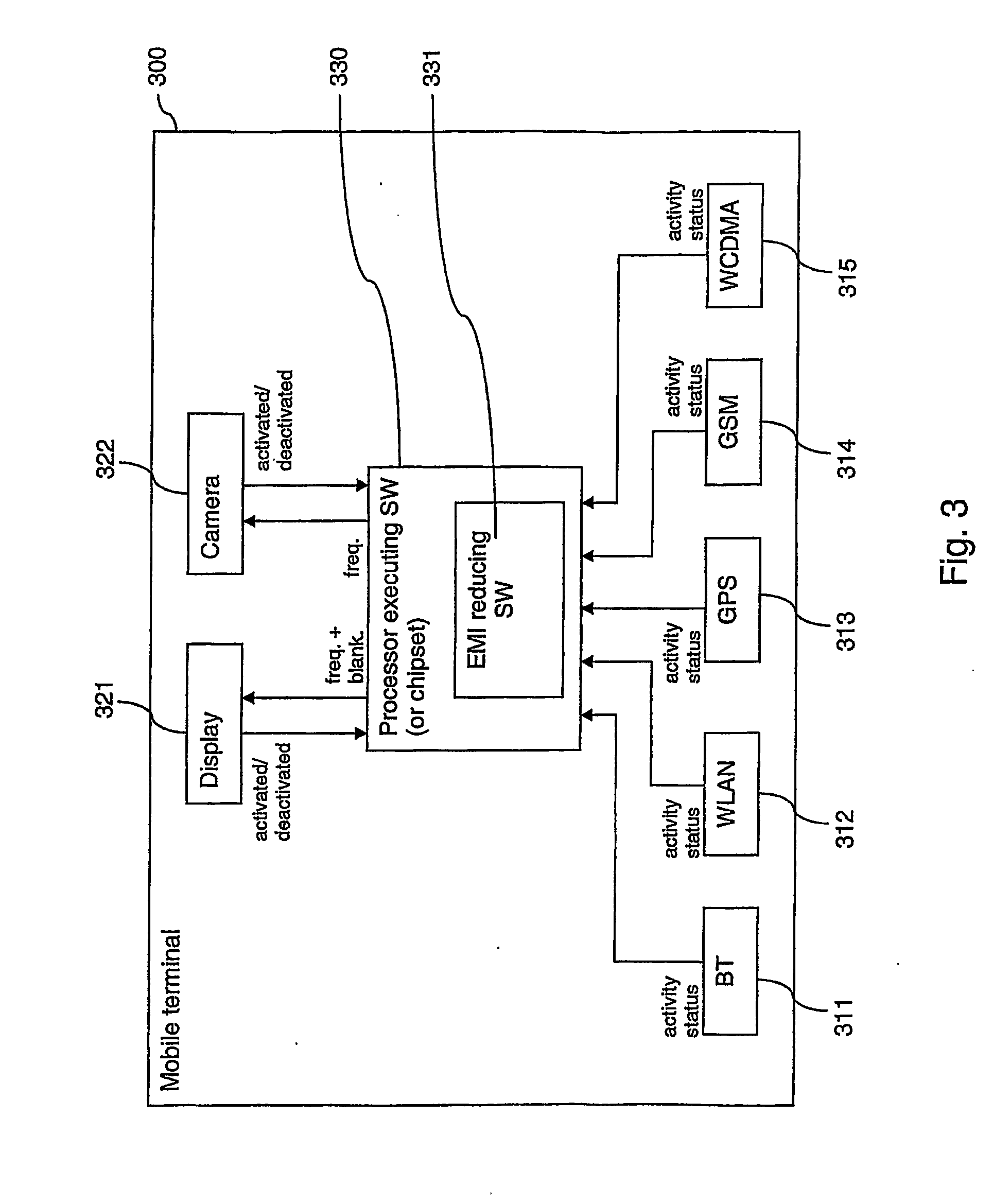
[0039]FIG. 3 is a schematic block diagram of an exemplary electronic device, which enables a protection of components from electromagnetic interferences in accordance with an embodiment of the invention.

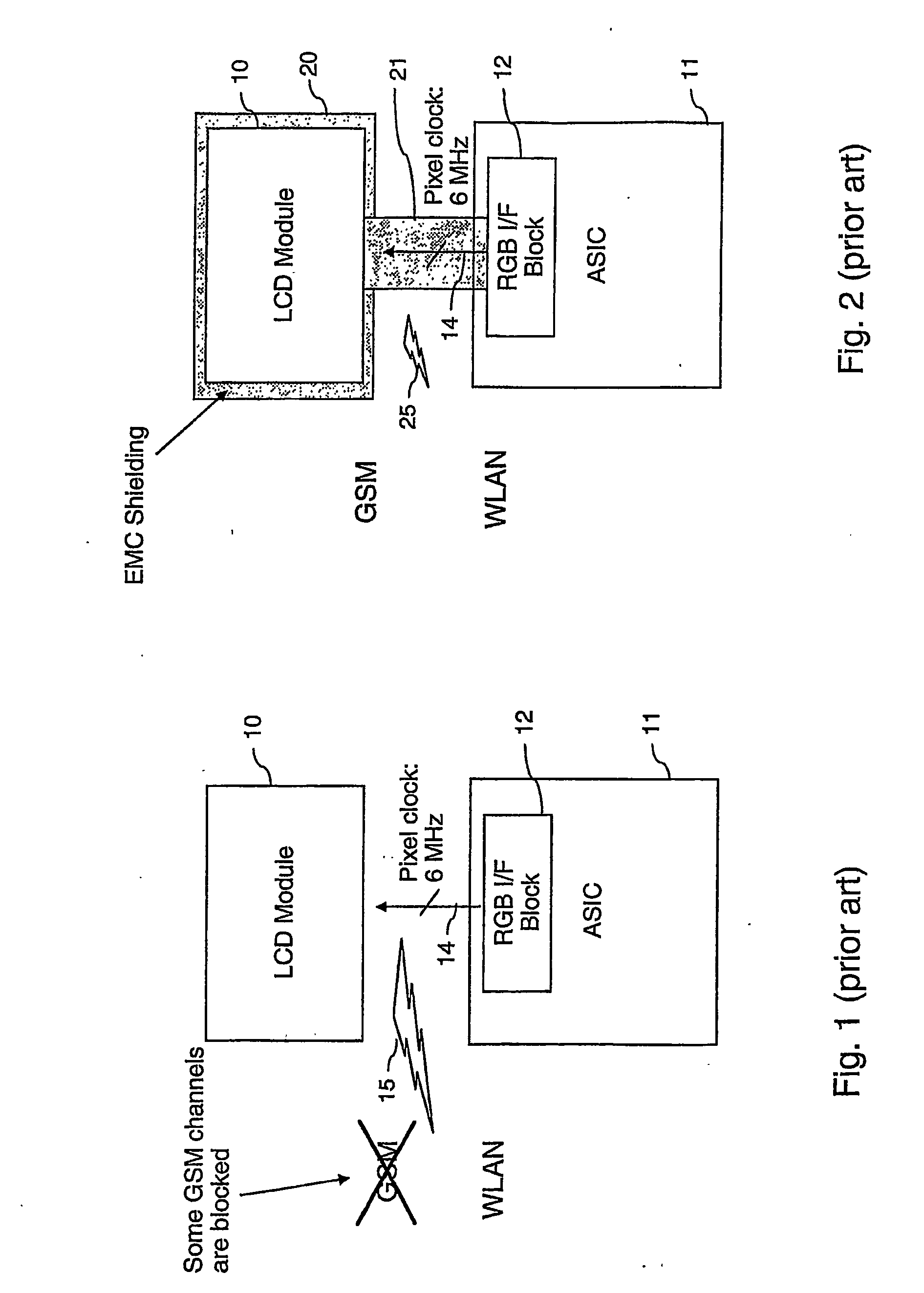
[0040] The electronic device is a mobile terminal 300. It comprises a first group of components for a respective radio system, including a Bluetooth™ (BT) component 311, a WLAN component 312, a GPS component 313, a GSM component 314 and a WCDMA component 315. All components of the first group operate in known frequency ranges, including for example a respective baseband frequency range, a respective intermediate frequency range and a respective radio frequency range. Further, the mobile terminal 300 comprises a second group of components including a display 321 and a camera module 322. The second group of components makes use of a respective clock signal for synchronizing the component internal operations. The clock signals are provided by a respective clock signal generator. The fr...


PUM


Abstract

An electronic device 300 comprises a processing component 330 for reducing electromagnetic interferences. The processing component 330 is adapted to determine an activity status of at least one first component 311-315 operating in at least one known frequency range. The processing component 330 is further adapted to adjust an operating frequency of an active second component 321-322 depending on the determined activity status of the at least one first component 311-315. The invention relates equally to a chipset 330, to a method, to a software code 331 and to a software program product realizing the functions of the processing component 330.

Description

FIELD OF THE INVENTION [0001] The invention relates to an electronic device reducing electromagnetic interferences. The invention relates equally to a chipset, to a method, to a software program code and to a software program product for reducing electromagnetic interferences. BACKGROUND OF THE INVENTION [0002] An electronic device may comprise a multitude of components for offering different functions. Some of these components may be a source of electromagnetic interferences (EMI), while other components of the same device may be sensitive to electromagnetic interferences. [0003] A mobile terminal, for instance, may comprise on the one hand peripheral components, like a display and a camera, etc. Such components typically use a clock oscillator for clocking the component internal operations. As an unintentional side effect, the clock oscillator generates radio frequency signals, called spurious emissions, in particular at the operating frequency and its harmonics. [0004] A mobile t...

Claims


Application Information

Patent Timeline
Patent Type & Authority Applications(United States)
IPC IPC(8): H04B17/00
CPCH04B15/04
Inventor PANKINAHO, ILKKAVAISANEN, RISTOSAARINEN, KAJNURMI, JUHA H-P
Owner NOKIA CORP
Why Eureka
Try Eureka