Liquid crystal device and electronic apparatus

a liquid crystal device and electronic equipment technology, applied in the direction of driving belts, belts/chains/gears, instruments, etc., can solve the problems of reducing transmittance and the like, increasing brightness, and dark display areas, so as to reduce a portion of a domain area and reduce the effect of deterioration of transmittan

Inactive Publication Date: 2007-09-27
EPSON IMAGING DEVICES CORP
View PDF3 Cites 43 Cited by
  • Summary
  • Abstract
  • Description
  • Claims
  • Application Information

AI Technical Summary

Benefits of technology

[0012]An advantage of some aspects of the invention is that it provides a liquid crystal device of an FFS system having a pixel structure which makes it possible to reduce a portion of a domain area that results in deterioration of transmittance, and an electronic apparatus using the same.
[0018]Therefore, the slits provided in the second transparent electrode are formed in an elongated shape as compared with the comparative example described above. Accordingly, the setting number of the slit can be reduced in the state where the slits are evenly arranged in the entire second transparent electrode as compared with the comparative example described above. A domain area occurs in the vicinity of any one end among the two ends of the long side direction of each of the slits also in the liquid crystal device during liquid crystal is driven. However, the setting number of the slits provided in the second transparent electrode is being reduced as compared with the comparative example described above, so that a portion of the domain area can be reduced in accordance with the reduction. As a result, the deterioration of the transmittance can be prevented.

Problems solved by technology

For this reason, there is a problem in that liquid crystal molecules positioned in the upper side of the pixel electrode are not sufficiently driven, thereby reducing transmittance and the like.
Therefore, the brightness is deteriorated in the domain area resulting in a dark display area.
Accordingly, there is a problem in that the portion of the domain area which does not contribute to the brightness is increased and the transmittance of the liquid crystal device is seriously deteriorated as a result.
Therefore, brightness is deteriorated in the domain area resulting in a dark display area.
Accordingly, there is a problem in that the number of the portion of the domain area which does not contribute to the brightness is increased as the number of the slit provided in each of the sub pixels is increased as in the comparative example described above and the transmittance of the liquid crystal device is seriously deteriorated as a result.

Method used


Image

  • Liquid crystal device and electronic apparatus
  • Liquid crystal device and electronic apparatus
  • Liquid crystal device and electronic apparatus

Examples


first embodiment

Structure of Liquid Crystal Device

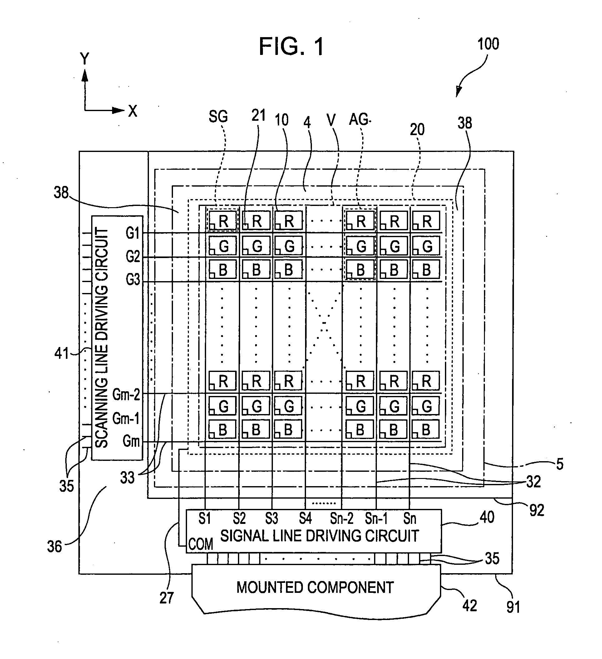
[0043]First, a structure of a liquid crystal device 100 according to a first embodiment of the invention will be described with reference to FIG. 1.

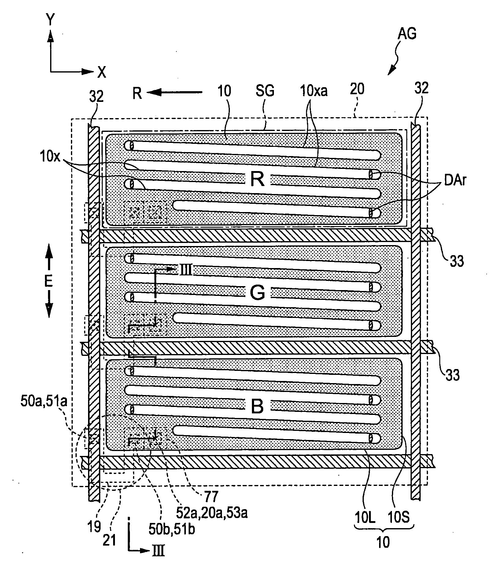
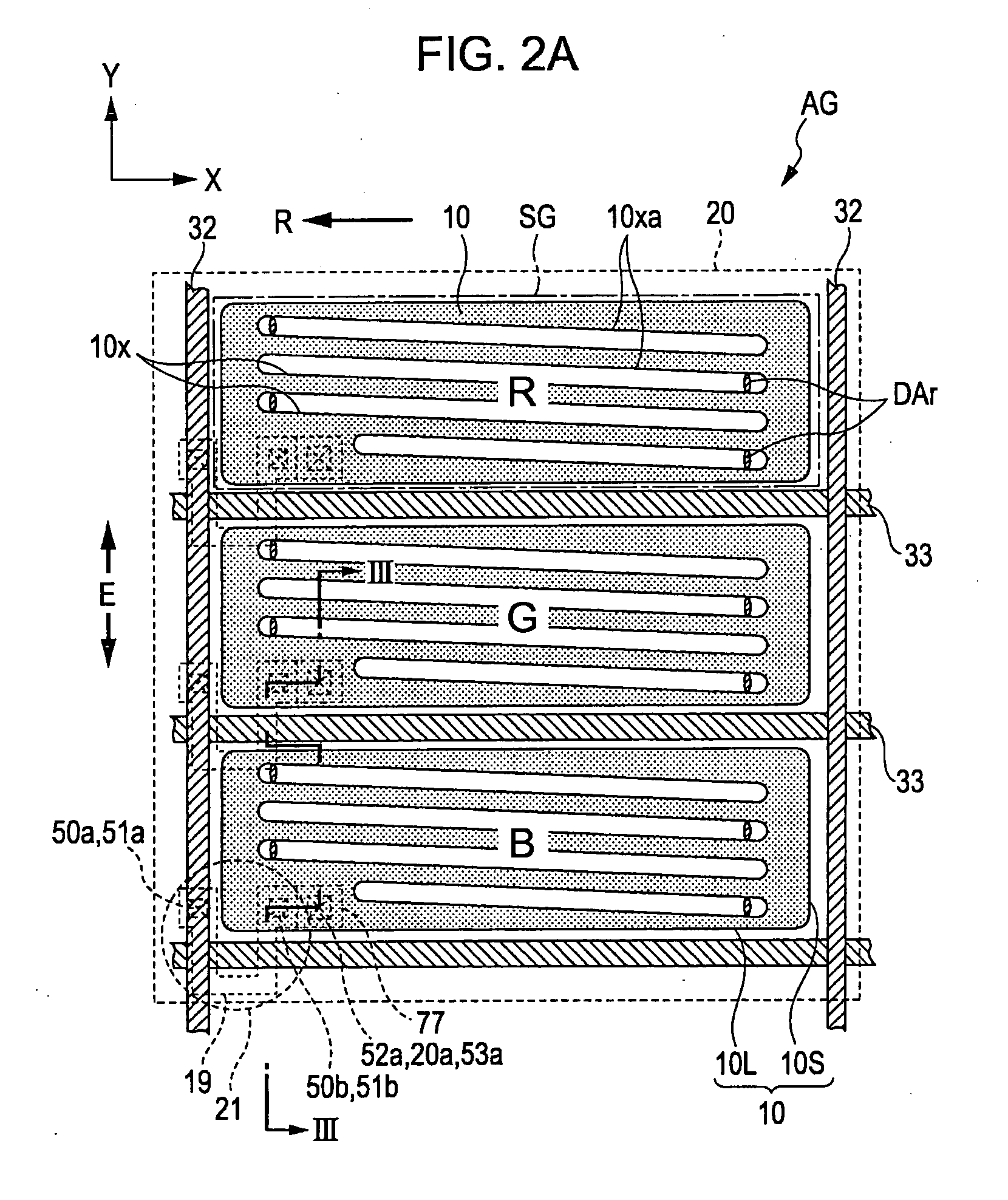
[0044]FIG. 1 is a plan view schematically showing a structure of the liquid crystal device 100 according to the first embodiment of the invention. A color filter substrate 92 is disposed at the front side of the plane of FIG. 1 (observation side), on the other hand, an element substrate 91 is disposed at the back side of the plane of FIG. 1. Note that the longitudinal direction of the figure (column direction) is defined as a Y direction and the lateral direction of the figure is defined as an X direction (row direction). Moreover, in FIG. 1, a region corresponding to one of an R, G, or B color is defined as one sub pixel area SG and one pixel area AG is composed of one of each R, G, and B color sub pixel areas AG aligned in one column and taking up three rows. Here, each sub pixel area SG is a horizonta...

second embodiment

[0119]A liquid crystal device 200 according to the second embodiment of the invention will now be described with reference to FIGS. 2B and 4.

[0120]FIG. 2B shows a planar structure of one pixel in element substrate 93 according to the second embodiment. Note that only the minimum number of elements for need in description are shown in FIG. 2B. FIG. 4 shows a cross-sectional view taken along the section line IV-IV in FIG. 2B and shows a cross-sectional structure including one sub pixel when sectioned at the position which passes through the LTPS type TFT elements 21.

[0121]When the second embodiment and the first embodiment are compared, mainly the positional relationship of the common electrode 20 and the pixel electrode 10 with respect to the third insulating layer 53 which is a dielectric layer is reversed in the element substrate. However, the other structure is the same in the both embodiments. Accordingly, hereinafter, like reference numerals are attached to the same elements as ...


PUM

PropertyMeasurementUnit
temperatureaaaaaaaaaa
thickness d1aaaaaaaaaa
thicknessaaaaaaaaaa

Abstract

1. A liquid crystal device includes a substrate including unit pixels each composed of a plurality of sub pixels arranged in a plurality of rows and one column and having a long side in the row direction and a short side in the column direction, wherein the substrate includes switching elements, an insulating film provided on at least the upper side of each of the switching elements, at least one first transparent electrodes provided on the upper side of the insulating film, other insulating film provided on the upper side of the first transparent electrodes, and at least one second transparent electrode formed on the upper side of the other insulating film and having a plurality of slits formed for each of the sub pixels and generating an electric field, the electric field being generated between the first transparent electrode and the second transparent electrode through each of the slits, and the extending direction of the long side of each of the slits is defined in a direction not the same as the extending direction of the short side of the sub pixels.

Description

BACKGROUND[0001]1. Technical Field[0002]The present invention relates to a liquid crystal device and an electronic apparatus preferably used for displaying a variety of information.[0003]2. Related Art[0004]Display modes of liquid crystal are typically broadly classified into a TN (Twisted Nematic) system, a vertical alignment system intended to provide a wide viewing angle and a high contrast, a lateral electric field system, an example of witch is an IPS (In-Plane Switching) system or an FFS system (Fringe Field Switching), and the like.[0005]Among these systems, in the IPS system, the direction of an electric field applied to liquid crystal is defined in a direction approximately parallel to a substrate, so that this system is advantageous in that the viewing angle characteristic can be improved as compared with the TN system and the like.[0006]However, in such a liquid crystal device, a pixel electrode made of a transparent conductive material such as ITO (Indium Tin Oxide) and ...

Claims


Application Information

Patent Timeline
Patent Type & Authority Applications(United States)
IPC IPC(8): F16G1/28G02F1/1343
CPCG02F1/133707G02F2001/134372G02F2001/134318G02F1/134363G02F1/134318G02F1/134372
Inventor FUJITA, SHIN
Owner EPSON IMAGING DEVICES CORP
Why Eureka
Try Eureka