Method of manufacturing epitaxial silicon wafer

Active Publication Date: 2007-10-04
SUMCO TECHXIV
View PDF8 Cites 22 Cited by
  • Summary
  • Abstract
  • Description
  • Claims
  • Application Information

AI Technical Summary

Benefits of technology

[0010]In the present invention, a base silicon wafer to have both top and bottom surfaces processed to a mirror finish may be processed in a cleaning process preceding a heater process of the rapid thermal process (RTP) or an epitaxial growth process wherein the cleaning process may comprise the steps of processing the silicon wafer with a hydrofluoric acid (HF) and processing the same with deionized water (DIW) at the last stage. In a silicon wafer used for a state-of-art device, in particular, a double-mirror-finish wafer with two sides (i.e., top and bottom surfaces) processed to a mirror finish, the quality of the bottom surface such as cleanliness about particles and impurities, flatness, and micro-roughness is as important as that of the top surface.

Problems solved by technology

On the other hand, the bottom face of the silicon single crystal substrate has not been paid much attention to with respect to the features and characteristics or the treatment.
However, the present inventors have found that the above-mentioned assumption is not necessarily correct if the properties, in particular, the optical properties of the bottom surface are concerned.
However, since the silicon single crystal substrate is not processed with a hydrofluoric acid, the ozone oxide films are unnecessarily strong such that the effects in the following processes may be reduced or blocked.

Method used


Image

  • Method of manufacturing epitaxial silicon wafer
  • Method of manufacturing epitaxial silicon wafer
  • Method of manufacturing epitaxial silicon wafer

Examples


experimental example

(Experimental Example)

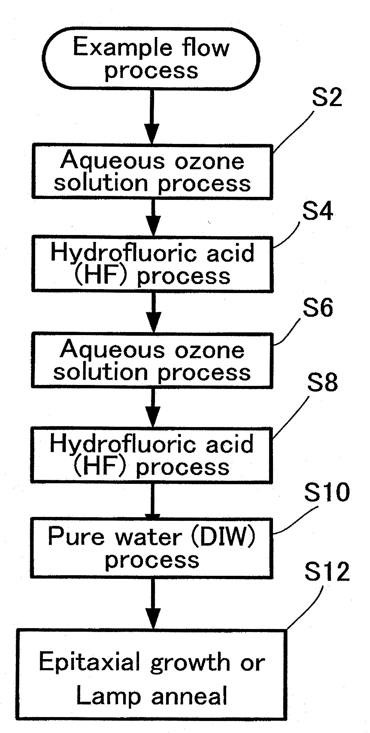
[0034]Now, details of the experimental examples that were actually made are explained. Silicon single crystal wafers having diameters of 200 mm and 300 mm were prepared as both surfaces of the respective wafers were processed to the mirror finish. These wafers were processed according to the flow charts as shown in FIGS. 3 and 4. Here, the process (S8) with the hydrofluoric acid (HF) was conducted by soaking the wafers into the approximately 1% dilute hydrofluoric acid for several to several tens seconds. Also, the process (S10) with the pure water (DIW) was conducted by showering the pure water onto the silicon wafer such that the wafer was rinsed with the pure water. In the step S12, the epitaxial growth was conducted under the aforementioned condition. Here, the aforementioned hydrofluoric acid process (S8) was also conducted by the spin cleaning as the approximately 1% of dilute hydrofluoric acid was showered onto the bottom surface of the silicon wafer. Th...


PUM


Abstract

A role of a bottom face of a silicon wafer is identified in a manufacturing process of the silicon wafer. And preferable characteristic feature is also identified. In order to obtain the above characteristic feature, a process method to be implemented into the method of manufacturing a normal silicon wafer is provided. For example, the method comprises: a pre-cleaning process for cleaning the silicon wafer having top and bottom faces processed to a mirror finish; and a rapid thermal process or an epitaxial growth process, wherein the pre-cleaning process comprises a hydrofluoric acid (HF) process and a subsequent pure water (DIW) process.

Description

CROSS REFERENCE TO RELATED APPLICATIONS[0001]This application is based upon and claims the benefits of priority from Japanese Patent Application No. 2006-100921 filed on Mar. 31, 2006, the entire contents of which are incorporated herein by reference.[0002]1. Field of the Invention[0003]The present invention relates to a method of manufacturing a silicon wafer. And more specifically, it relates to a method of cleaning the silicon wafer.[0004]2. Related Art[0005]When a silicon epitaxial layer is formed on a top surface of a silicon single crystal substrate, for example, the silicon single crystal substrate which has been processed in a prescribed cleaning process is placed on a susceptor in a reaction chamber in which a vapor phase growth is conducted. And a natural oxide film formed on the top surface of the silicon single crystal substrate is removed by etching with hydrogen as the inside of the reaction chamber is heated (e.g., in a range from 1100 degree Celsius to 1200 degree Ce...

Claims


Application Information

Patent Timeline
IPC IPC(8): H01L29/06
CPCH01L21/02052H01L21/02381H01L21/68735H01L21/02658H01L21/02532
Inventor HAYASHIDA, KOICHIRONARAHARA, KAZUHIROKATO, HIROTAKA
Owner SUMCO TECHXIV
Why Eureka
Try Eureka