Semiconductor device and manufacturing method thereof
Inactive Publication Date: 2007-10-04
FUJITSU SEMICON LTD
View PDF15 Cites 44 Cited by
Summary
Abstract
Description
Claims
Application Information
AI Technical Summary
This helps you quickly interpret patents by identifying the three key elements:
Problems solved by technology
Method used
Benefits of technology
Benefits of technology
[0022]In view of the foregoing, it is an object of the present invention to provide a semiconductor device having high moisture resistance and high reliability. Another object of the present invention is to provide a method for manufacturing the semiconductor device.
Problems solved by technology
However, when a probe test is thus performed, mechanical injuries may occur in an electrode pad due to contact with a probe.
Further, the problem caused by such penetration of moisture from the outside may similarly occur as long as the semiconductor device having an electrode pad is used.
For example, there is a problem that migration of wiring materials easily occurs due to moisture which penetrates into the inside through an injured electrode pad.
Method used
Image
Click on the blue label to locate the original text in one second.
Reading with bidirectional positioning of images and text.
Examples
first embodiment
[0041]A first embodiment will be first described.
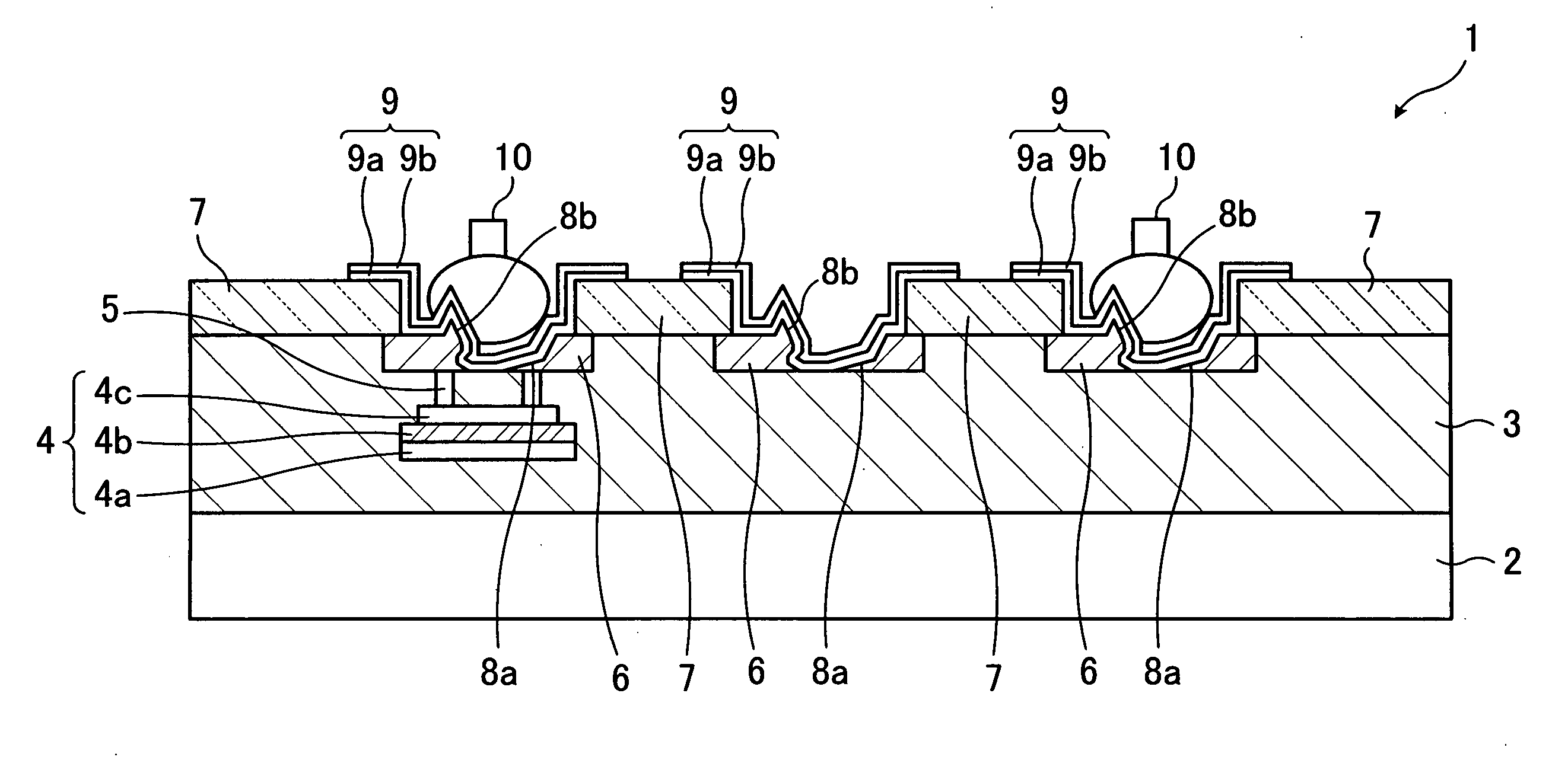
[0042]FIG. 1 is a schematic sectional view showing an essential part of a FeRAM element according to the first embodiment of the present invention.
[0043]A FeRAM element 1 shown in FIG. 1 has a ferroelectric capacitor 4 comprising a layered product including a lower electrode 4a made of platinum (Pt), a ferroelectric film 4b made of lead zirconate titanate (PZT), and an upper electrode 4c made of iridiumoxide (IrO2) within an interlayer insulating film 3 made of oxidesilicon (SiO2) formed over a semiconductor substrate 2.
[0044]In the FeRAM element 1, the ferroelectric capacitor 4 is electrically connected to a transistor (not shown) formed using the semiconductor substrate 2. To the element 1, a so-called stacked capacitor structure as described below is applied. That is, immediately above a conductive plug connected to the transistor, the ferroelectric capacitor 4 is provided to directly connect the conductive plug to the lower elec...
second embodiment
[0076]Next, a second embodiment will be described.
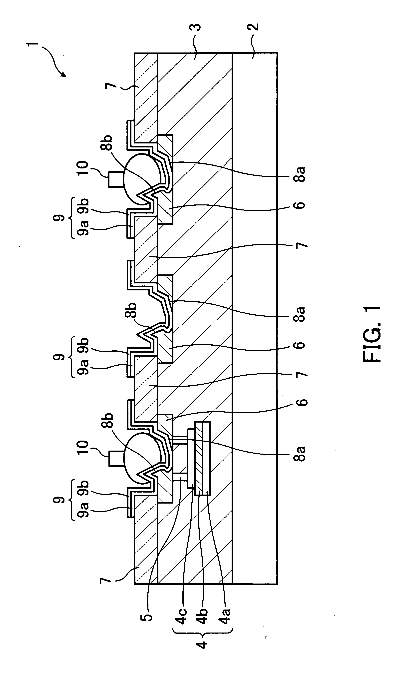
[0077]FIG. 3 is a schematic sectional view showing an essential part of a FeRAM element according to the second embodiment. In FIG. 3, the same elements as those shown in FIG. 1 are indicated by the same reference numerals as in FIG. 1 and the detailed description is omitted.
[0078]A FeRAM element 20 according to the second embodiment has the following structure. That is, the electrode pad 6 which is surfaced within the opening formed in the protective film 7 and is injured during a test using a probe, and the region from the electrode pad 6 to the opening outer periphery of the protective film 7 are covered with the metal film 9. Further, a metal bump 21 with a flat surface is formed over the film 9.
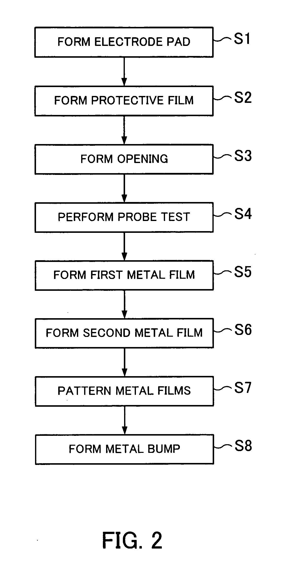
[0079]The FeRAM element 20 having such a structure is formed as follows. That is, after the probe test using the electrode pad 6, the metal film 9 composed of the first and second metal films 9a and 9b is formed over the electrode pad 6. ...
third embodiment
[0084]A FeRAM element 30 has the following structure. That is, the electrode pad 6 which is surfaced within the opening formed in the protective film 7 and is injured during a test using a probe, and the region from the electrode pad 6 to the opening outer periphery of the protective film 7 are covered with the metal film 9. Further, a solder bump 31 is formed on the film 9.
[0085]The FeRAM element 30 is formed as follows. That is, after the probe test using the electrode pad 6, the metal film 9 composed of the first and second metal films 9a and 9b is formed over the electrode pad 6. Then, the solder bump 31 with an approximately semicircular cross section is formed on the metal film 9 using a plating method or a printing method.
[0086]For the solder bump 31, for example, an alloy mainly containing tin (Sn) as well as an alloy containing lead (Pb) or indium (In) can be used. The solder bump 31 is formed such that an opening of the protective film 7 at a formation position of the bum...
PUM
Abstract
A semiconductor device and manufacturing method thereof improving moisture resistance of a FeRAM. After a probe test using a pad, a metal film is formed to cover the pad in an opening of a protective film and a region from the pad to an opening outer periphery of the protective film. On the metal film, a metal bump is formed. The metal film is formed to have a two-layer structure of the first and second metal films. Materials of the lower and upper layers are selected mainly in consideration of adhesion to the protective film and adhesion to the metal bump, respectively. Film formation conditions thereof are set to provide metal films with a desired quality and thickness. Thus, penetration of moisture from the pad or the periphery into a ferroelectric capacitor can be prevented and therefore, occurrence of potential inversion abnormalities due to penetrated moisture can be effectively suppressed.
Description
CROSS-REFERENCE TO RELATED APPLICATIONS[0001]This application is based upon and claims the benefits of priority from the prior Japanese Patent Application No. 2006-096633, filed on Mar. 31, 2006, the entire contents of which are incorporated herein by reference.BACKGROUND OF THE INVENTION[0002]1. Field of the Invention[0003]The present invention relates to a semiconductor device and a method for manufacturing the semiconductor device. More particularly, the present invention relates to a semiconductor device having a ferroelectric capacitor and a method for manufacturing the semiconductor device.[0004]2. Description of the Related Art[0005]A Ferro-electric Random Access Memory (FeRAM) element using a ferroelectric capacitive element (ferroelectric capacitor) as a storage capacitive element is a non-volatile memory device having the following characteristics. That is, a high-speed operation is enabled, power consumption is low and, writing and readout durability is excellent.[0006]In...
Claims
Application Information
Patent Timeline
Application Date:The date an application was filed.
Publication Date:The date a patent or application was officially published.
First Publication Date:The earliest publication date of a patent with the same application number.
Issue Date:Publication date of the patent grant document.
PCT Entry Date:The Entry date of PCT National Phase.
Estimated Expiry Date:The statutory expiry date of a patent right according to the Patent Law, and it is the longest term of protection that the patent right can achieve without the termination of the patent right due to other reasons(Term extension factor has been taken into account ).
Invalid Date:Actual expiry date is based on effective date or publication date of legal transaction data of invalid patent.

