Detection method of probe's tip location, storage medium storing the method, and probe device

Inactive Publication Date: 2007-10-04
TOKYO ELECTRON LTD
View PDF3 Cites 32 Cited by
  • Summary
  • Abstract
  • Description
  • Claims
  • Application Information

AI Technical Summary

Benefits of technology

[0029] In accordance with the aspects of the present invention, there can be provided a method for detecting tip positions of probes, a storage medium for storing the method and a probe device, the method

Problems solved by technology

In case the tip positions of the probes are detected by the camera, it takes a long time to focus the camera on the ends of the probes, thereby increasing time required to align the test object with the probe card.
However, in case of fine electrodes, parts of probes may not be properly aligned with the electrodes.
Further, since various probe cards are developed by a plurality of probe card makers, there are a need to develop a dedicated algorithm for recognizing three-dimensional images of the probes, which incurs considerable costs.
Further, although Reference 2 discloses therein that it is possible to check the pos

Method used


Image

  • Detection method of probe's tip location, storage medium storing the method, and probe device
  • Detection method of probe's tip location, storage medium storing the method, and probe device
  • Detection method of probe's tip location, storage medium storing the method, and probe device

Examples


first embodiment

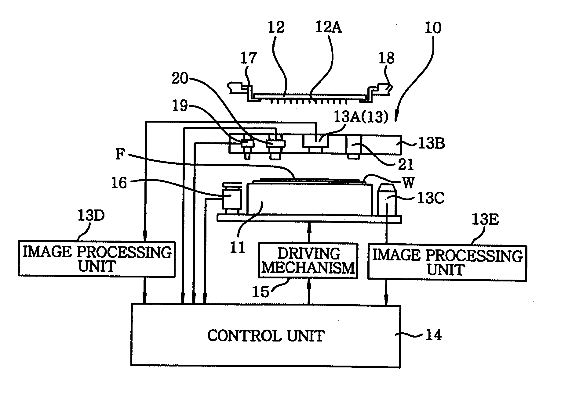
[0040] First of all, a probe device of the present invention will be described. As shown in FIG. 1, a probe device 10 of this embodiment includes a movable mounting table 11 for mounting thereon a wafer (not shown) serving as a test object; a probe card 12 disposed above the mounting table 11; an alignment mechanism 13 for aligning a plurality of probes 12A of the probe card 12 with the wafer on the mounting table 11; and a control unit 14 for controlling the mounting table 11, the alignment mechanism 13 and the like.

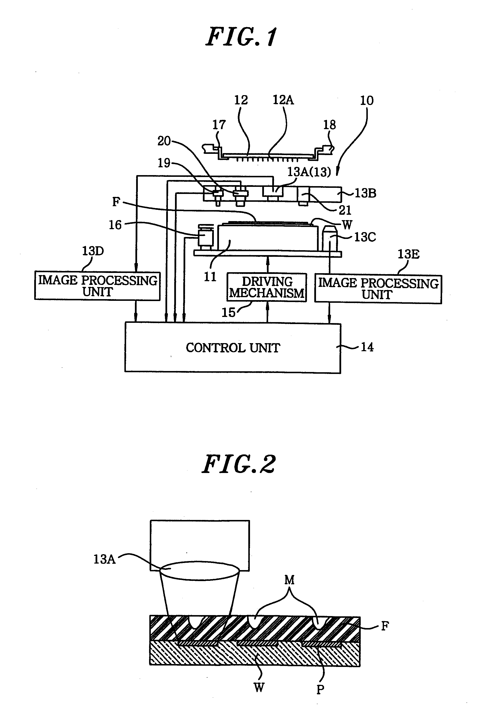
[0041] The alignment mechanism 13 is driven under the control of the control unit 14 to align the wafer on the mounting table 11 with the probes 12A of the probe card 12 and, then, the probes 12A and the wafer are made to electrically contact with each other for an electrical characteristic test of the wafer. In this embodiment, when detecting probe marks of the probes 12A, a substrate (test substrate) W having thereon a transparent film F is mounted, instead of the wa...

second embodiment

[0067] Although the first embodiment has the third step of measuring the surface height of the transparent film F by using the switch probe 19 and then detecting the positions of the probes, the second embodiment has a third step of measuring the surface height of the transparent film F by using a refractive index of the transparent film F and then detecting the positions of the probes. Since the second embodiment is same as the first embodiment except that the surface height of the transparent film F is obtained by using the refractive index of the transparent film F, the difference will be mainly explained hereinafter.

[0068] When the electrodes P of the test substrate W are detected through the transparent film F by the first CCD camera 13A, light is refracted by the transparent film F, as shown in FIGS. 2 and 6A, which hinders a detection of an actual surface height of the test substrate W. Therefore, the control unit 14 detects an apparent surface height of the test substrate W...

third embodiment

[0075] This embodiment has a feature in that a refractive index n of the transparent film F is obtained when it is unknown. In this case, since the refractive index n of the transparent film F is not known, the thickness L1 of the transparent film F and the correction value L2 of the height of the test substrate W need to be measured as can be seen from Eq. 1.

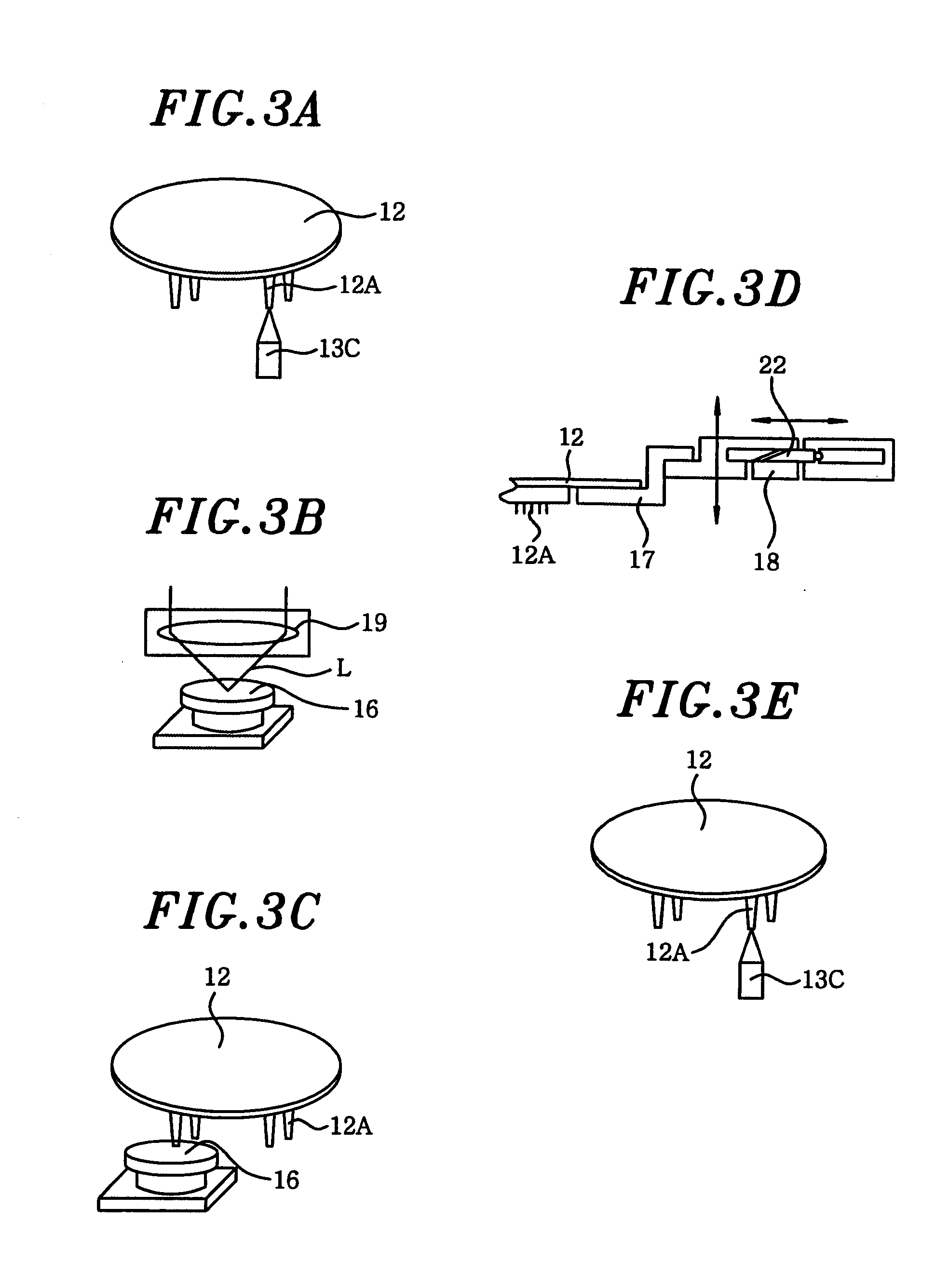
[0076] To do so, the correction value L2 on the height of the test substrate W needs to be obtained by using the first CCD camera 13A in accordance with the method shown in FIGS. 7A and 7B and, also, the thickness L1 of the transparent film F needs to be obtained by using the switch probe 19 in accordance with the method described with reference to FIGS. 8A and 8B. Since the numerical aperture of the first CCD camera 13A is known, tan ø can be obtained by substituting the known values in Eq. 1. The refractive index n (=sin ø / sin θ) of the transparent film F can be calculated based on tan θ and the equation, i.e., n=sin ø / sin θ...


PUM


Abstract

A method for detecting tip positions of probes which is performed prior to the wafer test includes a first step of attaching the transparent film F on the test substrate W having the electrodes P arranged same as those of the wafer; a second step of detecting the electrodes P of the test substrate W by using the first CCD camera 13A; a third step of detecting a surface height of the transparent film F; a fourth step of position-aligning the electrodes P of the test substrate W with the probes 12A. The method further includes a fifth step of forming the probe marks M on the transparent film F by making the probes 12A contact with the transparent film F; and a sixth step of detecting tip positions of the probes 12A based on the electrodes P of the test substrate W and the probe marks M.

Description

FIELD OF THE INVENTION [0001] The present invention relates to a method for detecting tip positions of probes in performing an electrical characteristic test of a test object such as a semiconductor wafer or the like, a storage medium for storing the method and a probe device; and, more particularly, to a method capable of detecting a plurality of tip positions of probes of a probe card with high precision and enhancing reliability of the test, a storage medium for storing the method and a probe device. BACKGROUND OF THE INVENTION [0002] When an electrical characteristic test of a test object such as a semiconductor wafer or the like is performed by using a probe card, for example, tip positions of probes of the probe card are detected by a camera for capturing images thereof and, then, the probes are made to contact with electrodes of the test object for the electrical characteristic test. In case the tip positions of the probes are detected by the camera, it takes a long time to f...

Claims


Application Information

Patent Timeline
IPC IPC(8): G01R31/02
CPCG01R31/2891H01L22/00
Inventor KOBAYASHI, MASAHITOHYAKUDOMI, TAKANORI
Owner TOKYO ELECTRON LTD
Why Eureka
Try Eureka