Processing method for wafer

a processing method and technology for wafers, applied in the direction of semiconductor/solid-state device manufacturing, basic electric elements, electric apparatus, etc., can solve the problems of difficult handling of semiconductor wafers, insufficient heat resistance of protective tapes, and easy cracking of semiconductor wafers, so as to improve handleability and durability, the effect of reducing the yield of semiconductor chips

Active Publication Date: 2007-10-04
DISCO CORP
View PDF3 Cites 21 Cited by
  • Summary
  • Abstract
  • Description
  • Claims
  • Application Information

AI Technical Summary

Benefits of technology

[0017]In another method example, the cutting tool moves relatively to the wafer parallel to the holding surface, so that the cutting tool cuts and removes at least the projection. In this method, in particular, the cutting tool may move parallel to an axial direction of the rotational shaft. In the relative movement, at least one of the cutting tool and the holding table may move parallel to the holding surface. In this case, while the wafer may be reciprocated, the cutting tool may be pressed on the top end surface of the projection, thereby cutting the projection. As a result, the projection can be removed efficiently.
[0018]In the wafer of which the projection of the peripheral reinforcing portion will be removed in the above processing method of the present invention, the rigidity can be secured by the peripheral reinforcing portion, so that

Problems solved by technology

Due to this, it is difficult to handle the semiconductor wafer after the thinning, and cracking easily occurs in the semiconductor wafer.
However, when a metal film composed of gold is provided by a method (for example, deposition or sputtering) on a rear surface of the semiconductor wafer after thinning, the protective tape has insufficient heat-resistance, so that the processing temperature needs to be lower.
Due to this, processing is more time-consuming in this case than in normal cases.
However, when the semiconductor wafer has the above peripheral reinforcing portion, it is difficult to stably hold the semiconductor wafer.
However, since this modification of the chuck table is not practical, the above peripheral reinforcing portion of the semiconductor wafer is r

Method used


Image

  • Processing method for wafer
  • Processing method for wafer
  • Processing method for wafer

Examples


Embodiment Construction

[0032]An embodiment of the present invention will be explained hereinafter with reference to the drawings.

1. Semiconductor Wafer

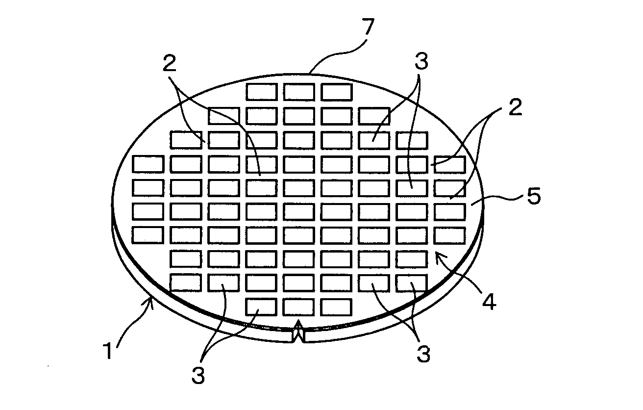
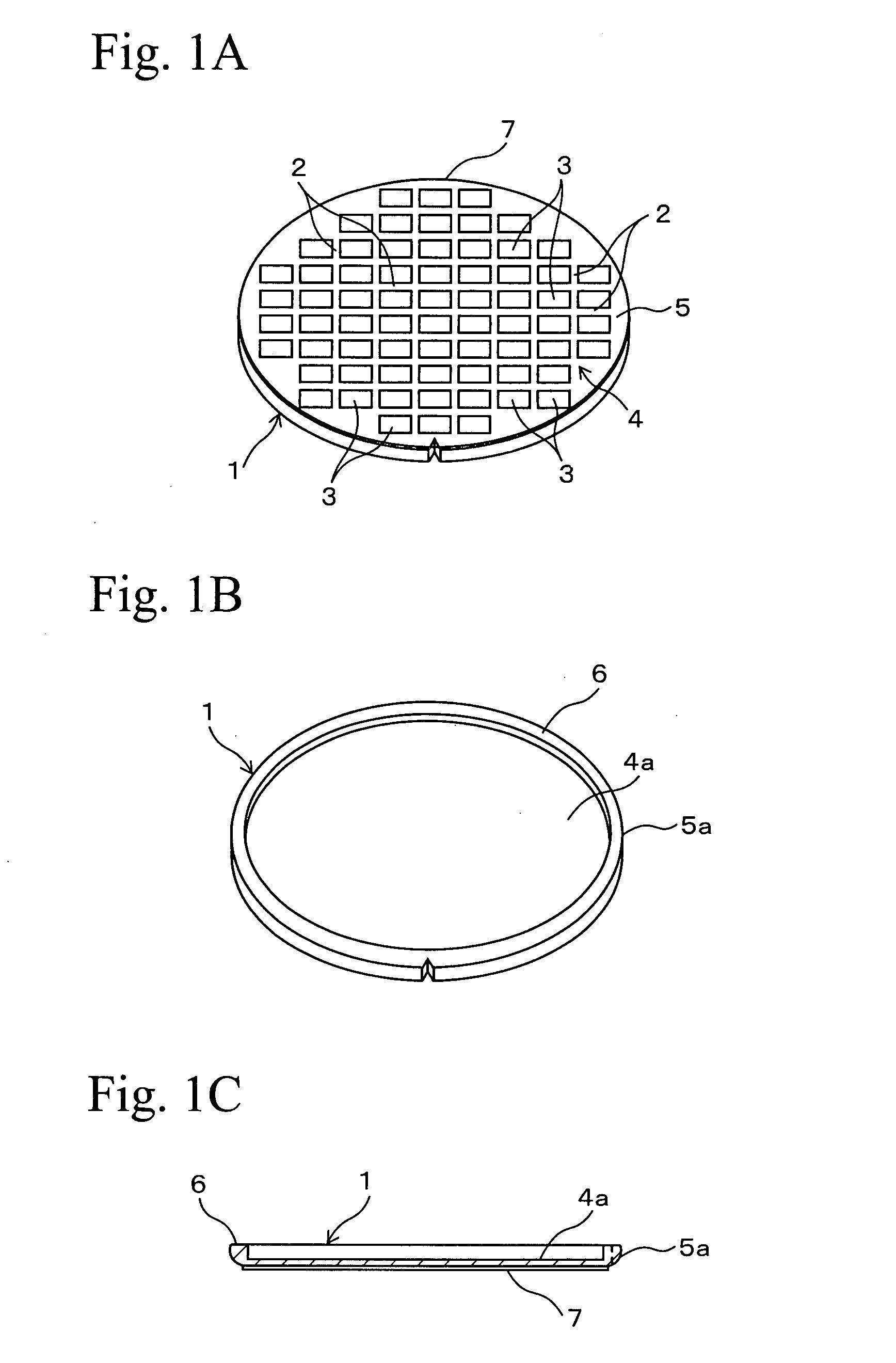
[0033]In FIGS. 1A to 1C, reference numeral 1 denotes a disc-shaped semiconductor wafer (hereinafter referred to simply as “wafer”) which is processed in the embodiment. The wafer 1 is a silicon wafer or the like. As shown in FIG. 1A, grid-like predetermined division lines 2 are formed on a surface of the wafer 1, and plural rectangular semiconductor chips 3 are defined by the predetermined division lines 2 on the surface of the wafer 1. Electronic circuits (for example, Integrated Circuits (ICs) and Large Scale Integrations (LSIs)), which are not shown in FIGS. 1A to 1C, are formed on surfaces of the semiconductor chips 3. The plural semiconductor chips 3 are formed on a device region 4 which is almost circular so as to be concentric with the wafer 1. A ring-shaped peripheral extra region 5, which has no semiconductor chip 3 formed thereon, is formed around...


PUM


Abstract

A processing method for a wafer includes: preparing a wafer which has a device region having plural devices formed on a surface of the wafer; and a peripheral reinforcing portion which is integrally formed around the device region and has a projection projecting outwardly on a rear surface of the wafer. The processing method further includes: holding the wafer on a holding surface of a rotatable holding table such that the rear surface of the wafer is exposed and the surface of the wafer closely contacts the holding table. The processing method further includes: thinning the peripheral reinforcing portion by cutting and removing at least the projection of the peripheral reinforcing portion of the wafer by using a cutting tool having a rotational shaft parallel to the holding surface, while rotating the wafer by rotating the holding table after the holding of the wafer. The peripheral reinforcing portion is thinned so as to have a thickness equal to or thinner than that of the device region by the thinning.

Description

[0001]This application claims priority under 35 U.S.C. §119 to Japanese Patent Application No. JP2006-090097 filed Mar. 29, 2006, the entire content of which is hereby incorporated by reference.BACKGROUND OF THE INVENTION[0002]1. Field of the Invention[0003]The present invention relates to a processing method in which a peripheral reinforcing portion of a wafer (for example, a semiconductor wafer), which is formed around a device region of the wafer having devices (for example, semiconductor chips) formed thereon and is thicker than the device region, is removed from the wafer.[0004]2. Description of the Related Art[0005]In general, semiconductor chips, which are used in various electronic apparatuses, are produced by the following method. That is, grid-like rectangular regions are defined by predetermined division lines on a disc-shaped semiconductor wafer, and electronic circuits are formed on surfaces of the rectangular regions. Next, a rear surface of the wafer is ground so as t...

Claims


Application Information

Patent Timeline
IPC IPC(8): H01L21/00
CPCH01L21/67092H01L21/68707H01L21/67132
Inventor KAJIYAMA, KEIICHIMASUDA, TAKATOSHI
Owner DISCO CORP
Why Eureka
Try Eureka