

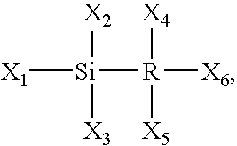
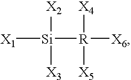
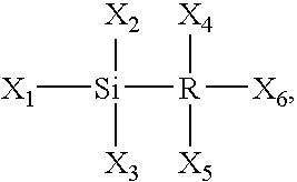
Silicon-containing layer deposition with silicon compounds
a technology of silicon compounds and silicon compounds, applied in the direction of crystal growth process, crystal growth process, polycrystalline material growth, etc., can solve the problems of toxic conditions and hazards often associated with etchant us
- Summary
- Abstract
- Description
- Claims
- Application Information
AI Technical Summary
Benefits of technology
Problems solved by technology
Method used
Image

Examples
example 1
Monocrystalline Silicon by Selective CVD
[0059] A substrate, Si, was employed to investigate selective, monocrystalline film growth by CVD. A silicon oxide feature existed on the surface of the wafer. The wafer was prepared by subjecting to a 0.5% HF dip for 30 seconds followed by baking at 750° C. for 60 seconds. The wafer was loaded into the deposition chamber (Epi CENTURA® chamber) and subjected to a hydrogen purge for 2 minutes. A flow of carrier gas, hydrogen, was directed towards the substrate and the source compounds were added to the carrier flow. The silicon compound, 30 sccm of Cl3SiSiH3, was delivered to the chamber at 10 Torr and 750° C. The substrate was maintained at 750° C. Deposition was carried out for 3 minutes to form a 400 Å epitaxial layer on the silicon surface, but no epitaxial growth occurred on the silicon dioxide surface.
example 2
Monocrystalline Silicon by Blanket CVD
[0060] A substrate, Si, was employed to investigate blanket, monocrystalline film growth by CVD. A silicon oxide feature existed on the surface of the wafer. The wafer was prepared by subjecting to a 0.5% HF dip for 30 seconds followed by baking at 750° C. for 60 seconds. The wafer was loaded into the deposition chamber (Epi CENTURA® chamber) and subjected to a hydrogen purge for 2 minutes. A flow of carrier gas, hydrogen, was directed towards the substrate and the source compounds were added to the carrier flow. The silicon compound, 50 sccm of Cl3SiSiH3, was added to the chamber at 100 Torr and 650° C. The substrate was maintained at 650° C. Deposition was carried out for 4 minutes to form a 1,600 Å epitaxial layer.
example 3
Polysilicon by CVD
[0061] The substrate was prepared as in Example 2. The wafer was loaded into the deposition chamber (POLYGEN™ chamber) and subjected to a hydrogen purge for 2 minutes. A flow of carrier gas, hydrogen, was directed towards the substrate and the source compounds were added to the carrier flow. The silicon compound, 100 sccm of HF2SiSiClH2, was added to the chamber at 80 Torr and 550° C. The substrate was maintained at 550° C. Deposition was carried out for 3 minutes to form a 1,200 Å layer.
PUM
| Property | Measurement | Unit |
|---|---|---|
| temperature | aaaaa | aaaaa |
| temperature | aaaaa | aaaaa |
| temperature | aaaaa | aaaaa |
Abstract
Description
Claims
Application Information