
Image display device

a display device and image technology, applied in the direction of discharge tubes/lamp details, discharge tubes/lamp details, cathode ray tubes/electron beam tubes, etc., can solve the problems of preventing the increase of display life, and the interior of the display panel is not sufficiently subject to gas release, etc., to achieve good mechanical strength and display quality, good quality and brightness

Inactive Publication Date: 2007-10-18
HITACHI DISPLAYS
View PDF4 Cites 0 Cited by
  • Summary
  • Abstract
  • Description
  • Claims
  • Application Information

AI Technical Summary

Benefits of technology

[0017]In consideration thereof, the present invention is proposed to solve the above problems, and an object thereof is to provide an image display device that can offer images with good quality and brightness with the increased mechanical strength and display quality of a display panel by optimizing the configuration of the display panel based on the screen size, i.e., the length, the placement interval, and the number of the spacers.
[0019]In the aspect of the invention, the configuration of the display panel is optimized based on the screen size, i.e., the length, the placement interval, and the number of the spacers. Such configuration optimization favorably leads to the satisfactorily excellent effect, e.g., the display panel is increased in mechanical strength and display quality, and the resulting image display is of good quality and brightness.
[0020]Also in the aspect of the invention, an internal gas smoothly flows between a plurality of space keeping members in the horizontal and longitudinal directions. This accordingly works well for the residual gas inside of the display panel so that the gas contamination is reduced in the electron source. The resulting image display thus shows excellent electron emission properties, and can be of high in image quality and brightness. This configuration leads to a satisfactorily excellent effect of achieving an image display device with long life, good quality, and high reliability.
[0021]Also in the aspect of the invention, the space keeping members are overlaid on the scanning signal electrodes, and are disposed along the same direction as the scanning signal electrodes. This configuration leads to a satisfactorily excellent effect of protecting the electrode components, e.g., electron source and image signal electrode, from any damage.

Problems solved by technology

The problem with such an FPD is that, because the space between the substrates is set to minimum, i.e., about 3 mm, an adhesive member for use to fix the spacers often does not serve enough for gas release.
This is one cause of a difficulty in keeping high the degree of vacuum, thereby preventing the increase of display life.
Another problem with such an FPD is that the interior of the display panel is not sufficiently subjected to gas release when sealed under a reduced pressure by heating in a sealing process, or at the time of vacuum exhaustion in an exhaustion process.
Such not-sufficient gas release resultantly causes gas contamination, thereby degrading the electron emission properties of an electron emission source.
Especially the gas between the spacers is hard to release.

Method used


Image

  • Image display device
  • Image display device
  • Image display device

Examples


first embodiment

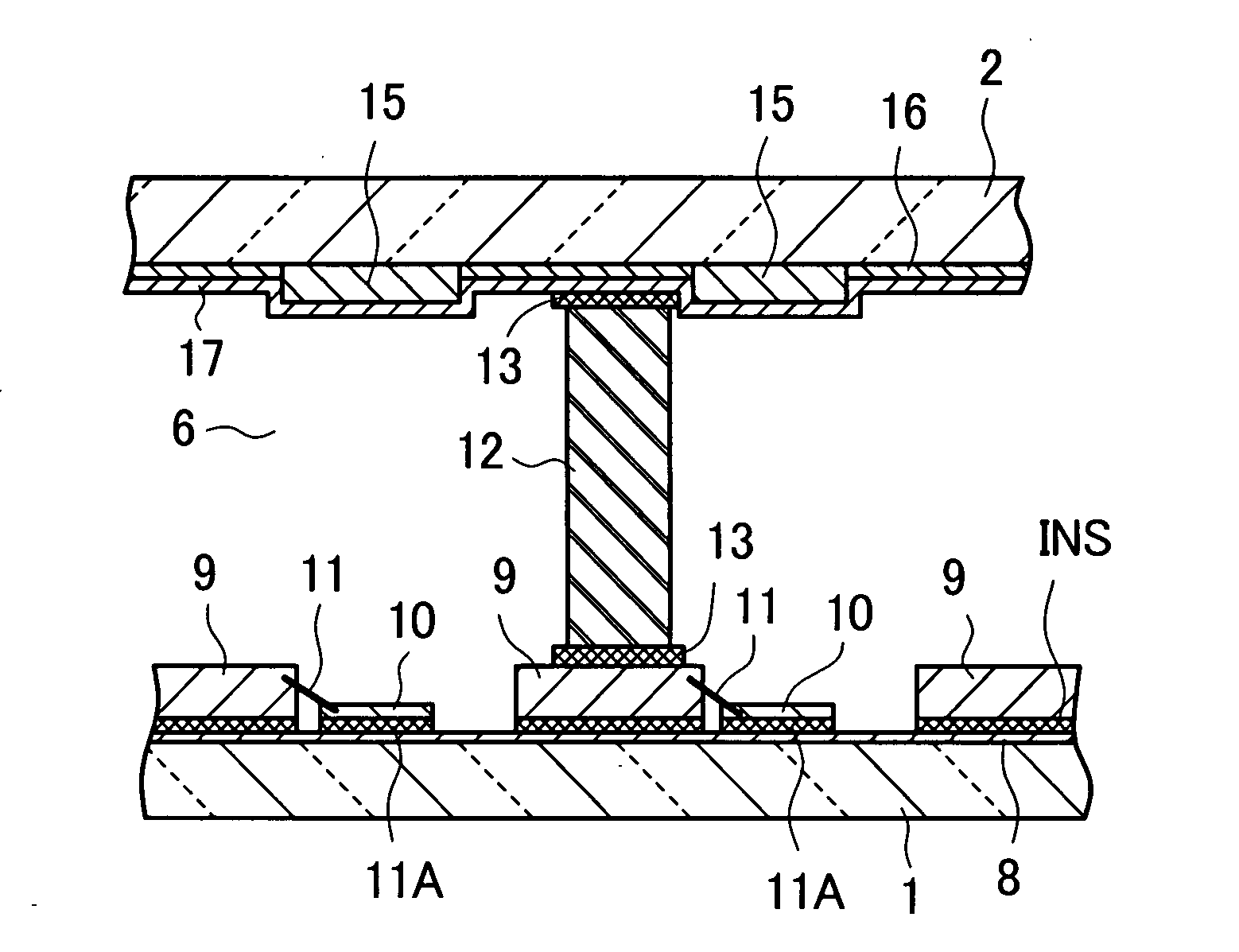
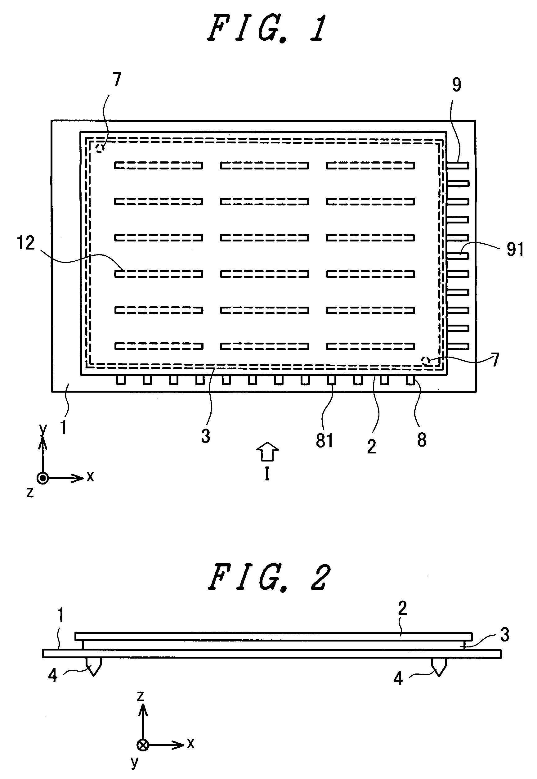
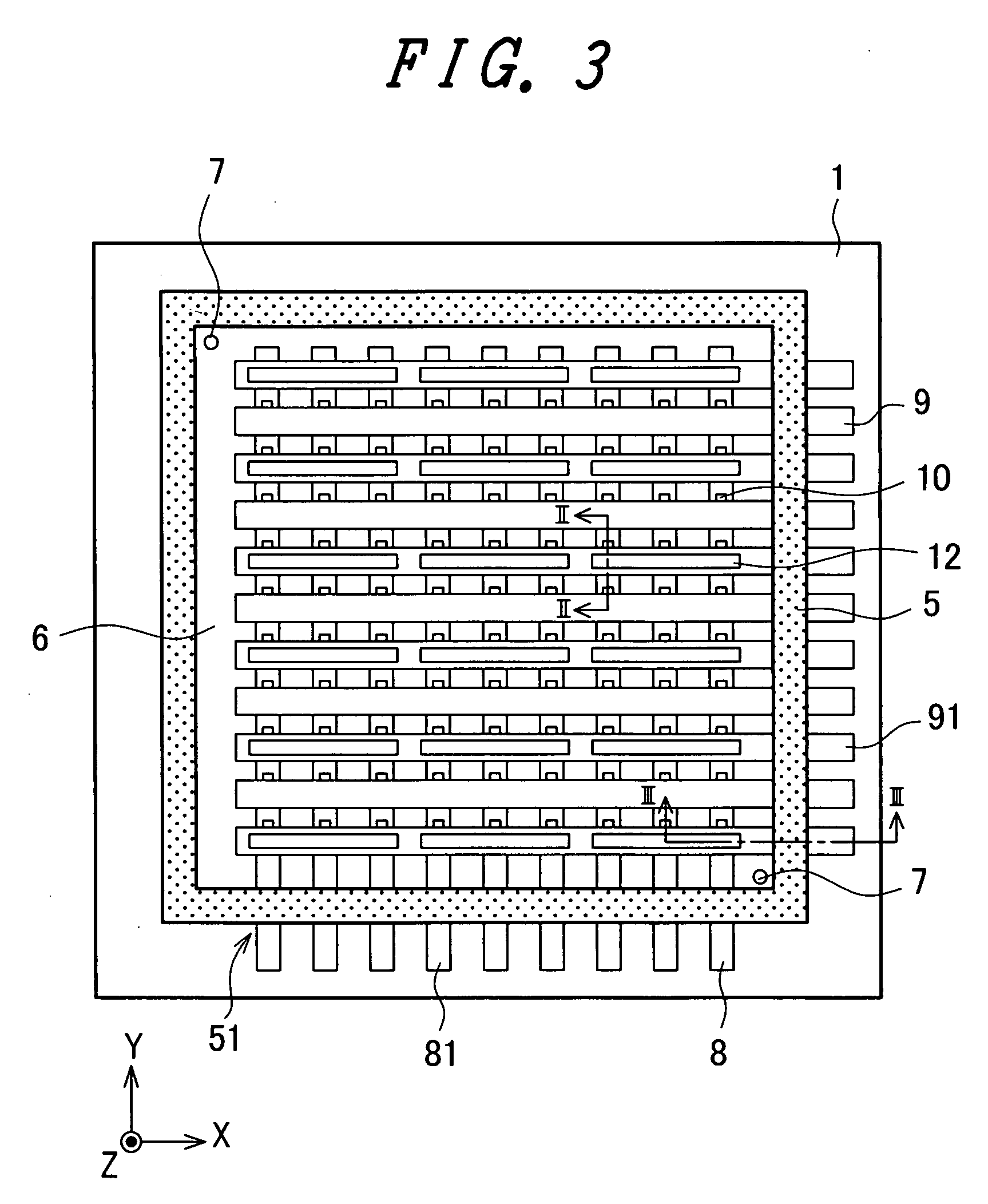
[0036]FIGS. 1 to 6 are each a diagram for illustrating an exemplary image display device of the invention. FIG. 1 is a plan view of an image display device, viewed from the side of a front substrate. FIG. 2 is a side view of the image display device of FIG. 1, viewed from an I direction. FIG. 3 is a schematic plan view of a rear substrate with no front substrate of FIG. 1. FIG. 4 is an overall perspective view showing the entire configuration of the image display device. FIG. 5 is a schematic enlarged cross sectional view of the rear substrate cut along a line II-II of FIG. 3, and the corresponding front substrate. FIG. 6 is a schematic enlarged cross sectional view of the rear and front substrates cut along a line III-III of FIG. 3.

[0037]In FIGS. 1 to 6, reference numerals 1 and 2 denote a rear substrate and a front substrate, respectively. The rear and front substrates 1 and 2 are each a glass plate with the thickness of about a few mm, e.g., about 3 mm. A reference numeral 3 deno...


PUM


Abstract

A plurality of spacers are so disposed as to satisfy the equations ofQx=(W+Gx+5) / (L+Gx)Gy=−1.5Gx+52.5Qy=H / Gy where a length needed for each of the spacers is L, a lateral length of the effective display area of the display panel is W, a vertical length of the effective display area of the display panel is H, the number of the spacers disposed in the lateral direction is Qx, the number of the spacers disposed in the vertical direction is Qy, a placement interval between any two of the spacers in the lateral direction is Gx, and a placement interval between any two of the spacers in the vertical direction is Gy. By optimizing the configuration of a display panel based on the screen size, i.e., the length, the placement interval, and the number of the spacers, the display panel is increased in mechanical strength and display quality so that the resulting image display device becomes able to offer images with good quality and brightness.

Description

BACKGROUND OF THE INVENTION[0001]1. Field of the Invention[0002]The present invention relates to a flat image display device utilizing electron emission into a vacuum space formed between front and rear substrates, more specifically, to an image display device equipped with a plurality of space keeping members between the front and rear substrates and, more in detail, to the placement configuration of the space keeping members.[0003]2. Description of the Related Art[0004]A color cathode-ray tube has been widely perceived as a display device excellent in brightness and definition. With the improved image quality achieved by the recent information processors and television broadcast, however, a demand is growing for a flat image display device (also referred to as flat panel display (FPD)) that is light in weight and occupies less space with the characteristics of high brightness and definition.[0005]To meet such a demand, as typical examples, a liquid crystal display device and a pla...

Claims


Application Information

Patent Timeline
Patent Type & Authority Applications(United States)
IPC IPC(8): H01J63/04H01J1/62
CPCH01J29/864H01J2329/866H01J2329/8625H01J31/127
Inventor ITO, HIROSHI
Owner HITACHI DISPLAYS
Learn More