
Oscillation circuit

a technology of oscillating circuits and oscillating signals, applied in the direction of oscillating generators, electrical devices, etc., can solve the problems of oscillating signal os

Inactive Publication Date: 2007-10-18
SEIKO EPSON CORP
View PDF4 Cites 2 Cited by
  • Summary
  • Abstract
  • Description
  • Claims
  • Application Information

AI Technical Summary

Benefits of technology

[0012]An advantage of the invention is to provide an oscillation circuit avoiding the above problem. According to an aspect of the invention, a oscillation circuit includes: a CMOS inverter coupled between a first potential and a second potential; a first element unit whose one terminal is coupled to an input terminal of the CMOS inverter; a second element unit whose one terminal is coupled to the input terminal of the CMOS inverter and whose other terminal is coupled to an output terminal of the CMOS inverter; a third element unit whose one terminal is coupled to the output terminal of the CMOS inverter; and a fourth element unit whose one terminal is coupled to the other terminal of the first element unit and to the other terminal of the third element unit, and whose other terminal is coupled to either the first potential or the second potential; in that: the first, second, third, and fourth element units are any of a quartz crystal resonator, a resistor, an inductor, and a capacitor, the oscillation circuit oscillating at a frequency determined by the first, second, and third element units.
[0013]Since the oscillation circuit of the invention includes the first, second, third, and fourth element units provided at positions as stated above, it is possible to prevent the chance of oscillation at frequencies other than a desired frequency and to make the waveform of the output oscillation frequency to be close to that of a sinusoidal wave.
[0014]It is preferable that the oscillation circuit be such that: the first and third element units are capacitors; the second element unit is a quartz crystal resonator; and the fourth element unit is a resistor.
[0015]It is preferable that the oscillation circuit be such that: the first element unit is a quartz crystal resonator; the second element unit is a capacitor; the third element unit is an inductor; and the fourth element unit is a resistor.
[0016]It is preferable that the oscillation circuit be such that: the first element unit is an inductor; the second element unit is a capacitor; the third element unit is a quartz crystal resonator; and the fourth element unit is a resistor.
[0017]It is preferable that the oscillation circuit be such that: the first and third element units are capacitors; the second element unit is a capacitor and an inductor connected serially to each other; and the fourth element unit is a quartz crystal resonator.

Problems solved by technology

Thus, there has been a problem that the wave of the oscillation signal OS100 does not become sinusoidal.

Method used


Image

  • Oscillation circuit
  • Oscillation circuit
  • Oscillation circuit

Examples


example 1

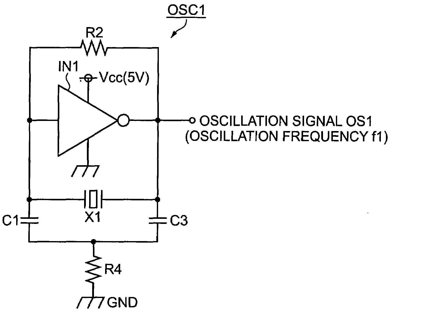
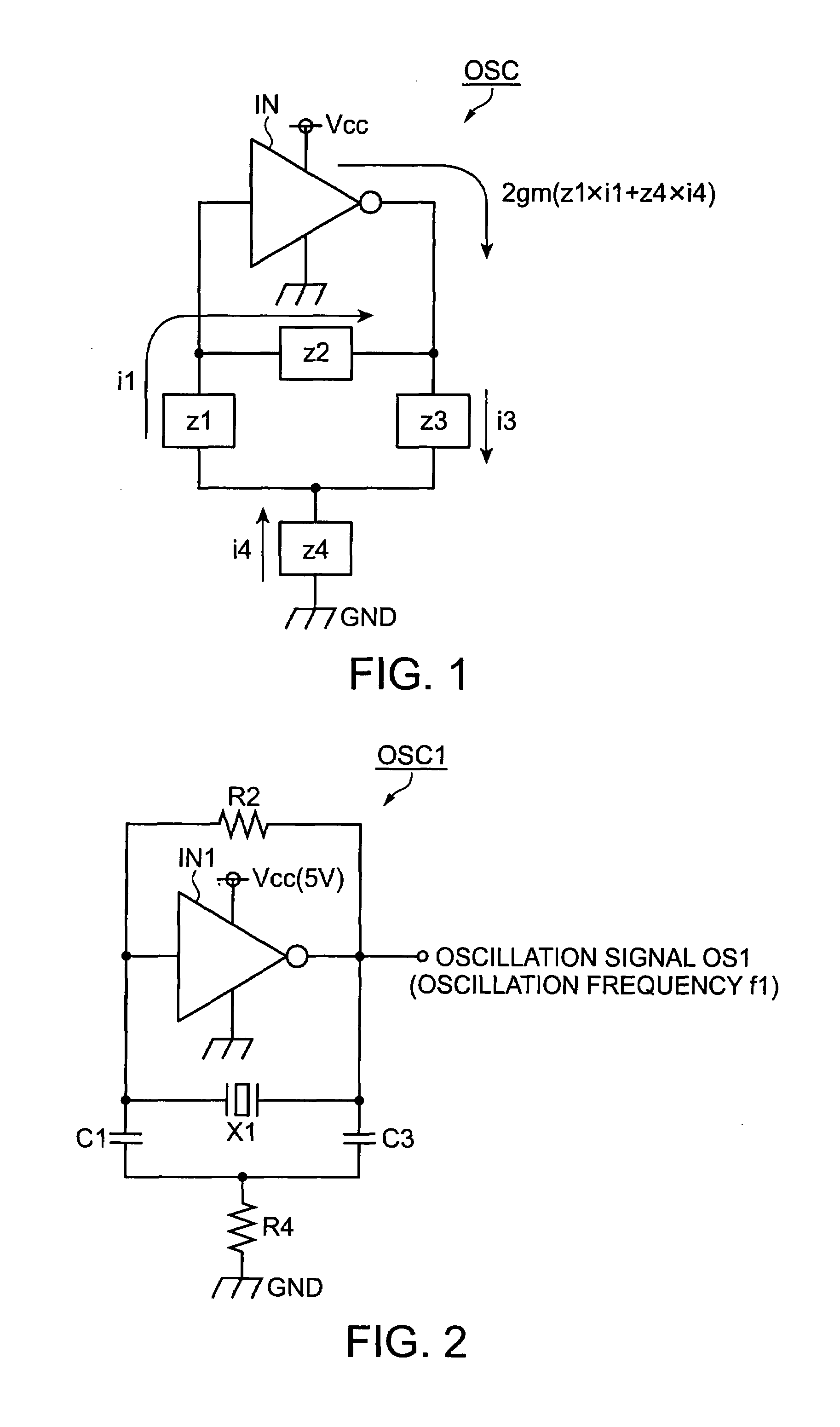
[0063]Referring to FIG. 2, an oscillation circuit OSC1 of an example 1 includes, as the inverter IN and the first to fourth impedances z1 to z4 of the oscillation circuit OSC of FIG. 1, an inverter IN1, a capacitor C1, a quartz crystal oscillator X1, a capacitor C3, and a resistor R4, and also includes a resistor R2 as a bias resistance.

[0064]The first to fourth impedances z1 to z4 are defined as shown in equations 18. When the equations 18 are substituted into the equation 12 that is the basic formula for z2=zxt, an equation 19 is given. Also, when the equation 19 is solved with respect to a circuit resistance Rc and a circuit capacitance Cc, equations 20 are given.

Equation  18z1=1jω.C1z2=zxtz3=1jω.C3z4=R4(18)Equation  19zxt+1jω.(1C1+1C3)-1ω2C1C3×112gm+R4=Rc+1jω.Cc=0(19)Equation  20Rc=-1ω2C1C3×112gm+R41Cc=1C1+1C3(20)

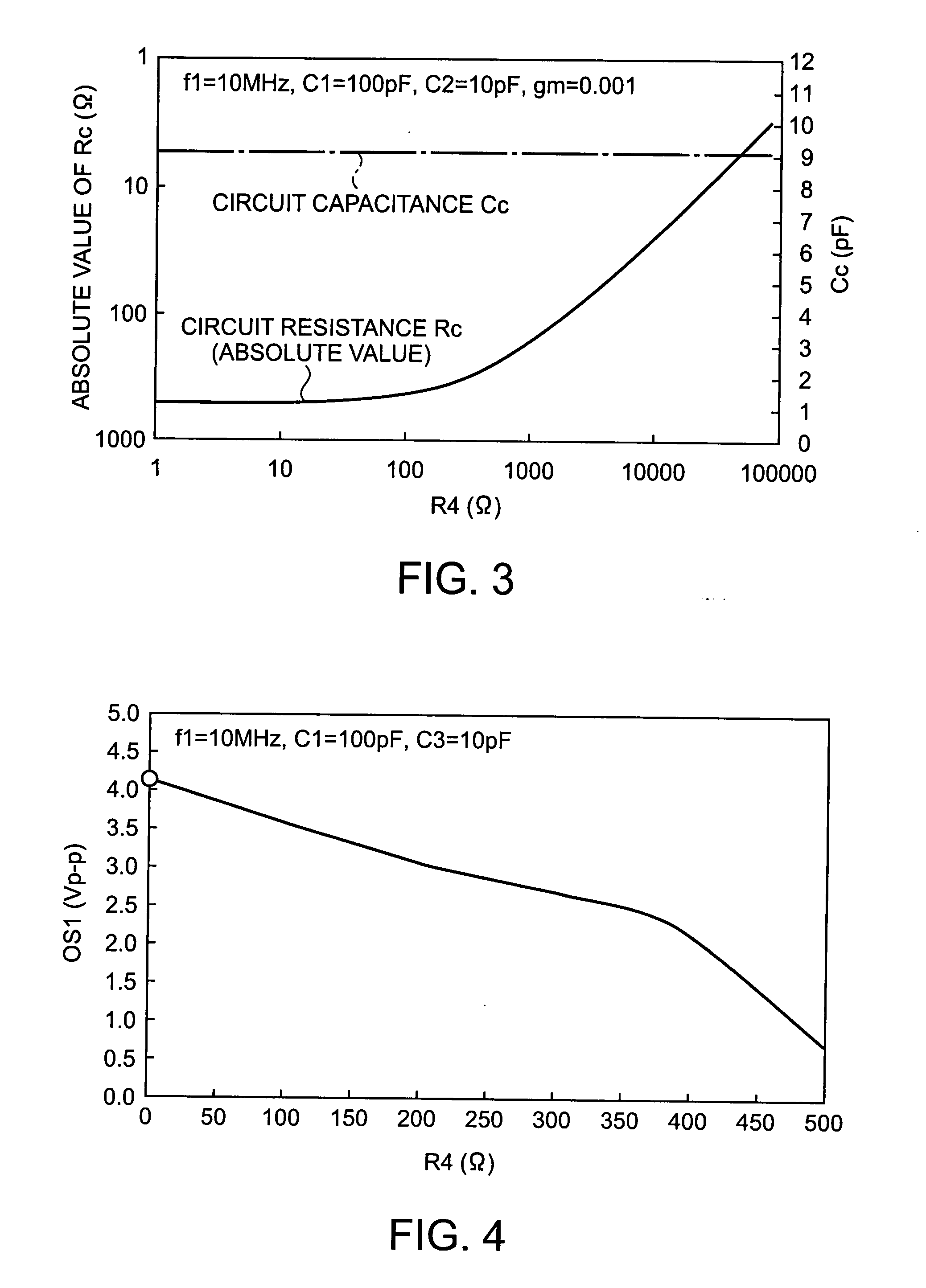
[0065]Pertaining to the equations 20 of the oscillation circuit OSC1 of the example 1, when a simulation is performed provided that the oscillation frequency f1 of an o...

example 2

[0067]With reference to FIG. 6, an oscillation circuit OSC2 of an example 2 includes, as the inverter IN and the first to fourth impedances z1 to z4 of the oscillation circuit OSC of FIG. 1, the inverter IN1, the quartz crystal oscillator X1, a capacitor C2, an inductor L3 and a bypass condenser Cp, and the resistor R4, and also includes the bias resistor R2.

[0068]The first to fourth impedances z1 to z4 in this case are defined as shown in equations 21. When the equations 21 are substituted into the equation 14 that is the basic formula for z1=zxt, an equation 22 is given. Also, when the equation 22 is solved with respect to the circuit resistance Rc and the circuit capacitance Cc, equations 23 and 24 are given.

Equation  21z1=zxtz2=1jω.C2z3=jω.L3ω232=1C2L3z4=R4(21)Equation  22zxt-2gm(1+2gmR4)(2gmω2ω232)+{ω.C2(1+2gmR4)}2×(1-ω2ω232)ω2ω232+1jωω2.C2(1+2gmR4)2(2gmω2ω232)2+{ω.C2(1+2gmR4)}2×(1-ω2ω232)=zxt+Rc+1jω.Cc=0(22)Equation  23Rc=-2gm(1+2gmR4)(2gmω2ω232)2+{ω.C2(1+2gmR4)}2×(1-ω2ω232)ω2...

example 3

[0071]With reference to FIG. 10, an oscillation circuit OSC3 of an example 3 includes, as the inverter IN and the first to fourth impedances z1 to z4 of the oscillation circuit OSC of FIG. 1, the inverter IN1, an inductor L1 and the bypass condenser Cp, the capacitor C2, the quartz crystal oscillator X1, and the resistor R4, and also includes the bias resistor R2.

[0072]The circuit resistance Rc and the circuit capacitance Cc of the oscillation circuit OSC3 of the example 3 are given in the equations 23 and 24, as in the case with the circuit resistance Rc and the circuit capacitance Cc of the oscillation circuit OSC2 of the example 2.

[0073]FIG. 11 shows the experimental results of the oscillation circuit of the example 3. In this experiment, the oscillation frequency f3 of an oscillation signal OS3=10 MHz, the capacitor C2=10 pF, and the inductor L1=6 μH. Referring to FIG. 11, when the resistor R4 is greater than around 2,500 Ω, the oscillation signal OS3 becomes a good sinusoidal w...


PUM


Abstract

An oscillation circuit, including: a complementary metal oxide semiconductor (CMOS) inverter coupled between a first potential and a second potential; a first element unit whose one terminal is coupled to an input terminal of the CMOS inverter; a second element unit whose one terminal is coupled to the input terminal of the CMOS inverter and whose other terminal is coupled to an output terminal of the CMOS inverter; a third element unit whose one terminal is coupled to the output terminal of the CMOS inverter; and a fourth element unit whose one terminal is coupled to the other terminal of the first element unit and to the other terminal of the third element unit, and whose other terminal is coupled to either the first potential or the second potential; in that: the first, second, third, and fourth element units are any of a quartz crystal resonator, a resistor, an inductor, and a capacitor; the oscillation circuit oscillating at a frequency determined by the first, second, and third element units.

Description

BACKGROUND[0001]1. Technical Field[0002]The present invention relates to an oscillation circuit using a quartz crystal resonator.[0003]2. Related Art[0004]With reference to a circuit diagram of FIG. 24, an oscillation circuit OSC100 of the related art includes: a complementary metal oxide semiconductor (CMOS) inverter IN100, a quartz crystal resonator X100, resistors R100 (bias resistor) and R200, and capacitors C100 (the capacitance is C1) and C300 (the capacitance is C3). The oscillation circuit OSC100 outputs an oscillation signal OS100 having an oscillation frequency f100 that is determined by the quartz crystal resonator X100 and the capacitors C100, C300. Referring to a block diagram of FIG. 25, the oscillation circuit OSC100 is also expressed as an equivalent circuit including: the CMOS inverter IN100, the resistor R100 connected in parallel to the CMOS inverter IN100, an impedance z1 coupled between an input terminal of the CMOS inverter IN100 and a ground potential GND, an ...

Claims


Application Information

Patent Timeline
Patent Type & Authority Applications(United States)
IPC IPC(8): H03B5/32
CPCH03B5/364
Inventor SATO, TOMIO
Owner SEIKO EPSON CORP
Learn More