Method and structure for self aligned formation of a gate polysilicon layer

a polysilicon layer and gate technology, applied in the field of integrated circuits, can solve the problems of reducing the yield of integrated circuit devices, and reducing the cost of integrated circuit or chip fabrication facilities, so as to reduce process steps and facilitate use , the effect of increasing the yield of integrated circuits

Active Publication Date: 2007-10-18
SEMICON MFG INT (SHANGHAI) CORP
View PDF8 Cites 190 Cited by
  • Summary
  • Abstract
  • Description
  • Claims
  • Application Information

AI Technical Summary

Benefits of technology

[0009]Many benefits are achieved by way of the present invention over conventional techniques. For example, the present technique provides an easy to use process that relies upon conventional technology. In some embodiments, the method provides means to reduce process steps and higher device yields in dies per wafer. Additionally, the method provides a process that is compatible with conventional equipment and processes. Preferably, the method can be applied to a variety of applications such as memory, application specific integrated circuit, microprocessor, and others. Particularly, the invention provides a method to fabricate gate structures for integrated circuit devices. Depending on the embodiment, one or more of these benefits may be achieved. These and other benefits are described in more throughout the present specification and more particularly below.

Problems solved by technology

An integrated circuit or chip fabrication facility can cost hundreds of millions, or even billions, of U.S. dollars.
Making devices smaller is very challenging, as each process used in integrated fabrication has a limit.
Although there have been significant improvements, such method still have many limitations.
As merely an example, as these device designs become smaller and smaller, challenges exists in current lithography and etch processes.
Additionally, these gate designs are often difficult to manufacture and generally require complex manufacturing processes and structures, which lead to inefficiencies and may cause low device yields from leakages.

Method used


Image

  • Method and structure for self aligned formation of a gate polysilicon layer
  • Method and structure for self aligned formation of a gate polysilicon layer
  • Method and structure for self aligned formation of a gate polysilicon layer

Examples


Embodiment Construction

[0019]According to present invention, techniques including method for manufacturing of semiconductor devices are provided. More particularly, the invention provides a method for fabricating gate structures for memory devices. But it would be recognized that the invention has a much broader range of applicability. For example, the invention can be applied to application specific integrated circuit devices, logic devices, and others.

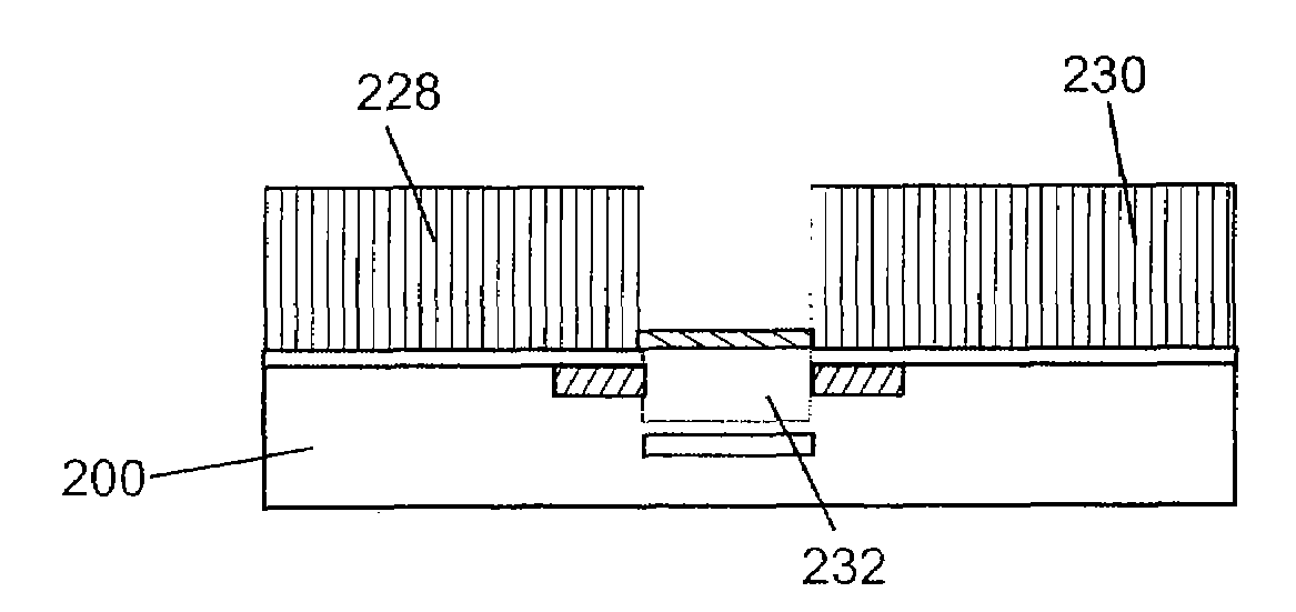
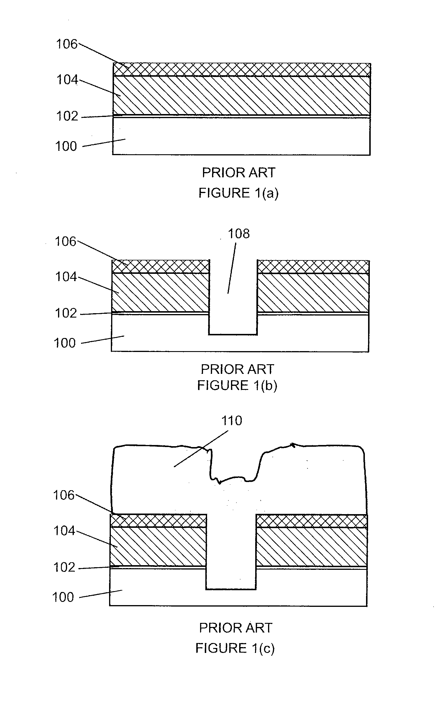
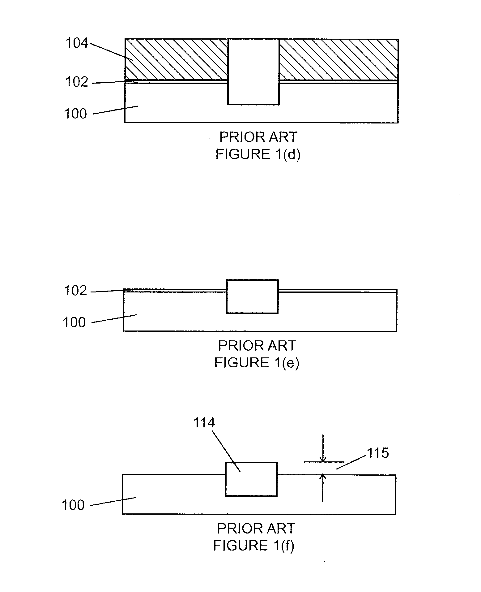
[0020]FIG. 1(a) to 1(q) are simplified diagrams illustrating a conventional method of fabricating gate structures for integrated circuit devices. As shown in FIG. 1(a), the conventional method includes providing a semiconductor substrate 100 having a surface. A dielectric stack is formed overlying the semiconductor substrate. The dielectric stack often comprises of silicon oxide 102, silicon nitride 104, and silicon oxynitride 106. The dielectric stack and a portion of the semiconductor substrate is subjected to a first masking and etch process to form a t...


PUM

PropertyMeasurementUnit
heightaaaaaaaaaa
heightaaaaaaaaaa
widthaaaaaaaaaa

Abstract

A method for processing semiconductor devices includes providing a semiconductor substrate. The method includes forming a pad oxide layer overlying the substrate and forming a silicon nitride layer overlying the pad oxide layer. The method includes forming a trench region extending through an entirety of a portion of the silicon nitride layer and extends into a depth of the semiconductor substrate. The method also includes filling the trench region with an oxide material. The oxide material extends from a bottom portion of the trench region to an upper surface of the silicon nitride layer. The method includes planarizing the oxide material and selectively removing the silicon nitride layer to form an isolation structure. A polysilicon material is deposited overlying the isolation structure. The polysilicon material is planarized to expose a top portion of the isolation structure and form a first electrode and a second electrode structures separated by a portion of the isolation structure.

Description

CROSS-REFERENCES TO RELATED APPLICATIONS[0001]This application claims priority to Chinese Application No. 200610025646.0; filed on Apr. 12, 2006; commonly assigned, and of which is hereby incorporated by reference for all purposes.BACKGROUND OF THE INVENTION[0002]The present invention is directed to integrated circuits and their processing for the manufacture of semiconductor devices. More particularly, the invention provides a method and structures for manufacturing gate structures for NOR flash memory integrated circuit devices, commonly called Flash devices. But it would be recognized that the invention has a much broader range of applicability.[0003]Integrated circuits have evolved from a handful of interconnected devices fabricated on a single chip of silicon to millions of devices. Conventional integrated circuits provide performance and complexity far beyond what was originally imagined. In order to achieve improvements in complexity and circuit density (i.e., the number of d...

Claims


Application Information

Patent Timeline
Patent Type & Authority Applications(United States)
IPC IPC(8): H01L21/336
CPCH01L21/26513H01L21/2652H01L21/76224H01L29/66825H01L27/11521H01L29/66545H01L27/115H10B69/00H10B41/30
Inventor JIANG, LISHAO, YINGPENG, LIBBERTWU, AUTER
Owner SEMICON MFG INT (SHANGHAI) CORP
Why Eureka
Try Eureka