Manufacture of printed circuit boards with stubless plated through-holes

a technology of printed circuit boards and through holes, applied in the field of process, can solve problems such as electrical performance, need to be removed, and detrimental effects on signal integrity

Active Publication Date: 2007-10-25
IBM CORP
View PDF13 Cites 37 Cited by
  • Summary
  • Abstract
  • Description
  • Claims
  • Application Information

AI Technical Summary

Problems solved by technology

Thus, regardless of which two copper interconnect layers in the PCB are associated with the through-hole, the copper is present throughout the hole, i.e. from top to bottom of the PCB as well as extra copper 30 (copper stubs) at the through-holes, which are known to have detrimental effects on signal integrity.
These extraneous copper stubs 30 limit the electrical performance of the copper interconnection especially at high frequency, and therefore, they often need to be removed.
The backdrilling process is time consuming, expensive and subjects the PCB to unnecessary damage, which affects the production yield.
First, the process is time consuming because each through-hole must be carefully drilled only to a limited depth which varies from hole-to-hole.
Third, some of the PCBs are damaged by the backdrilling and have to be discarded.

Method used


Image

  • Manufacture of printed circuit boards with stubless plated through-holes
  • Manufacture of printed circuit boards with stubless plated through-holes
  • Manufacture of printed circuit boards with stubless plated through-holes

Examples


Embodiment Construction

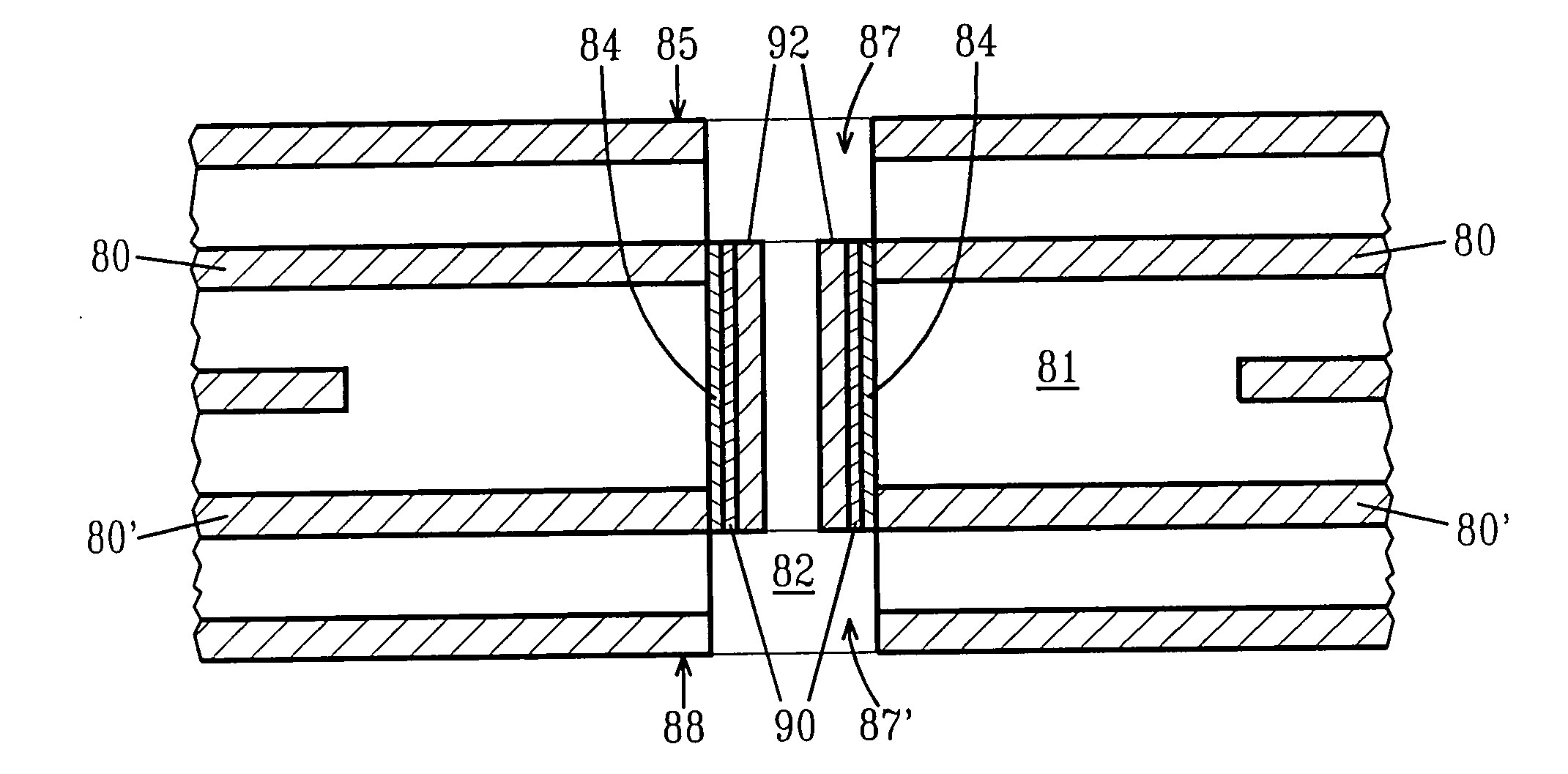
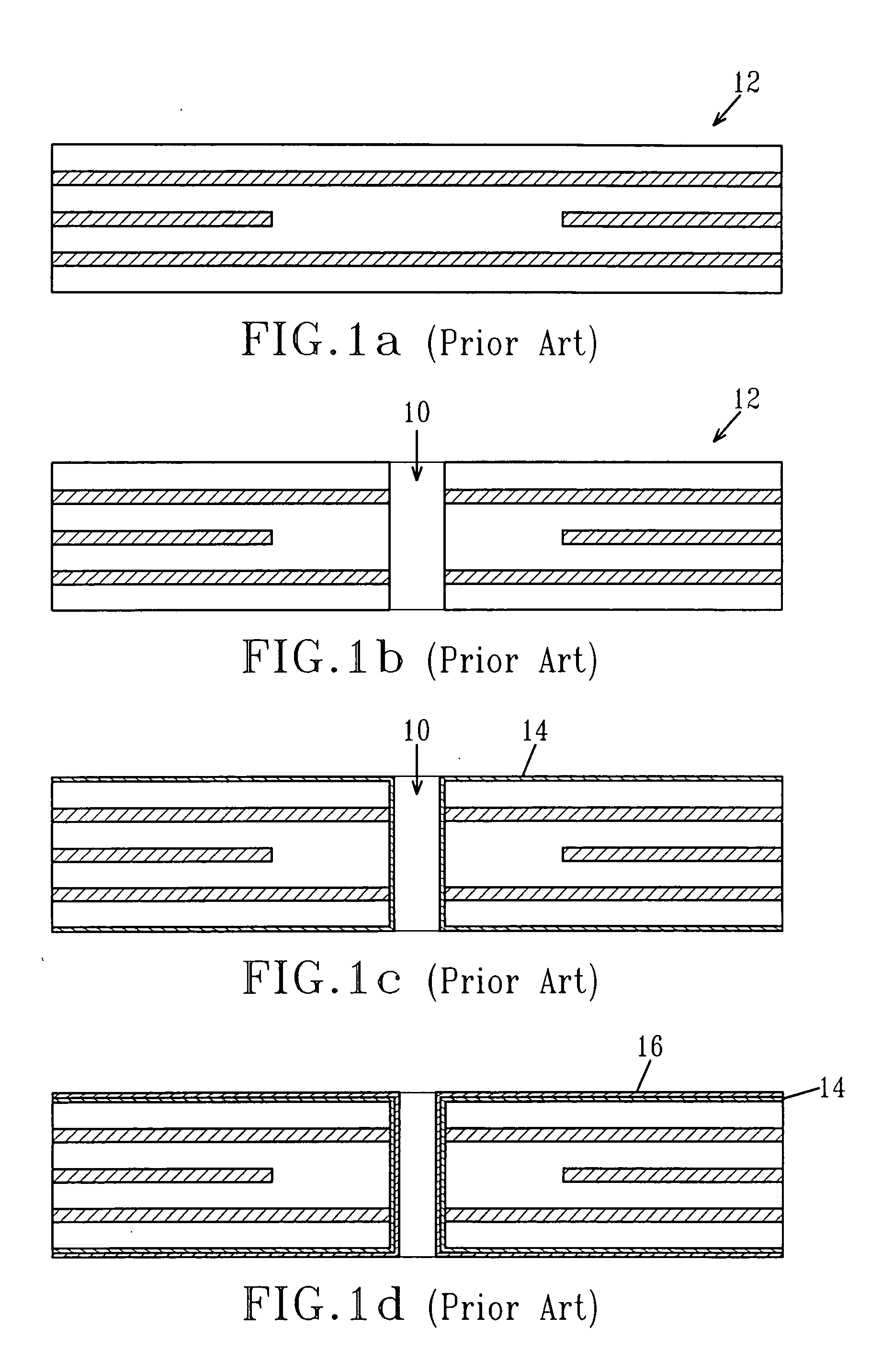
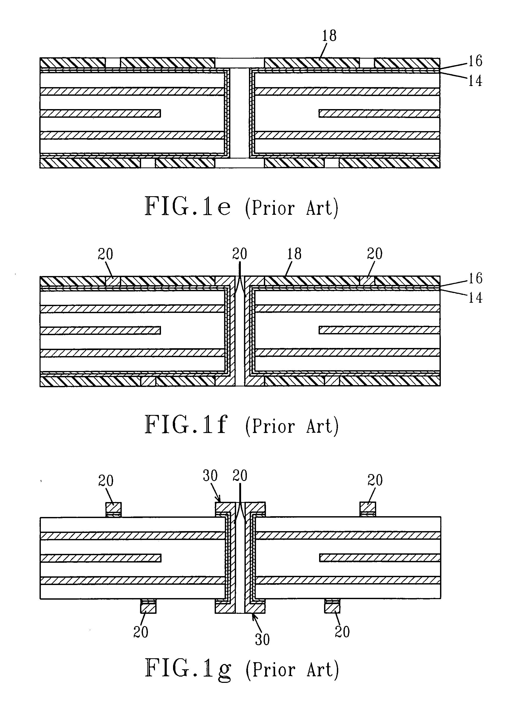
[0018] The invention is directed to a process of copper plating a through-hole in a printed circuit board. The process comprises providing a printed circuit board (PCB) with at least two copper interconnect lines separated by an insulator in the vertical direction, and providing a through-hole in the PCB in the vertical direction such that the interconnect lines provide a copper land in the through-hole. A seed layer is then applied to an interior surface of the through-hole. An outermost portion of the seed layer is then removed from the interior surface of the through-hole with a laser. Copper is then applied to the seed layer. The term vertical direction refers to the cross-sectional direction through the PCB, i.e., from the top external planar surface to the opposite (bottom), external planar surface of the PCB.

[0019] The step of applying copper can include an electroless process to form a first copper layer on the interior surface of the through-hole. The electroless copper de...


PUM

PropertyMeasurementUnit
areaaaaaaaaaaa
poweraaaaaaaaaa
diameteraaaaaaaaaa

Abstract

A process of copper plating a through-hole in a printed circuit board, and the printed circuit board made from such process. The process comprises: providing a printed circuit board with at least two copper interconnect lines separated by an insulator in the vertical direction; providing a through-hole in the printed circuit board in the vertical direction such that the interconnect lines provide a copper land in the through-hole; applying a seed layer to an interior surface of the through-hole; removing an outermost portion of the seed layer from the interior surface of the through-hole with a laser; applying copper on the seed layer.

Description

FIELD OF THE INVENTION [0001] This invention is directed to a process of making printed circuit boards by removing select portions of seed layer by laser ablation, and to printed circuit boards made by the process. BACKGROUND OF THE INVENTION [0002] Printed circuit boards (PCBs) are widely used to hold and electrically connect selected electronic components. Printed circuit boards are comprised of copper electrical interconnects separated by levels of insulating dielectric materials. In the horizontal xy plane, the copper interconnect lines are patterned on each of the individual layers and the layers joined to form a composite. Through-holes are then drilled in the vertical z direction from top to bottom of the composite, passing through each layer of the composite as well as through the copper landing pads on the layers to which electrical connection is required. A seed layer followed by one or more copper layers is then applied to the interior surface of the drilled through-holes...

Claims


Application Information

Patent Timeline
Patent Type & Authority Applications(United States)
IPC IPC(8): H01K3/10H05K1/16
CPCH05K1/0237Y10T29/49167H05K3/429H05K2201/09845H05K2203/0242H05K2203/175H05K1/0298H05K1/181H05K3/32Y10T29/4913Y10T29/49126Y10T29/49155Y10T29/49156Y10T29/49165Y10T29/49128H05K3/027
Inventor BUCHWALTER, STEPHEN L.BUDD, RUSSELL A.
Owner IBM CORP
Why Eureka
Try Eureka