Liquid Crystal Panel Using the Film Transistor and Manufacturing Methods of the Same

a technology of film transistors and liquid crystal panels, applied in the direction of instruments, maps/plans/charts, albums, etc., can solve the problems of leakage current, brightness, sharpness deterioration, etc., and achieve the effect of increasing sharpness

Inactive Publication Date: 2007-10-25
ILJIN DISPLAY
View PDF5 Cites 23 Cited by
  • Summary
  • Abstract
  • Description
  • Claims
  • Application Information

AI Technical Summary

Benefits of technology

[0011] It is therefore an object of the present invention to provide a liquid crystal panel using a thin film transistor and a manufacturing method thereof for forming a storage capacitor lower electrode under black matrices which increase sharpness by cutting off a reflected light, and for realizing a contact structure of electrically connecting the storage capacitor lower electrode with a drain electrode without loss of an active layer.

Problems solved by technology

As a result, sharpness may deteriorate.
Besides, when light is incoming to a channel part of the thin film transistor, the channel part of the thin film transistor creates an optical current, causing a leakage current.
However, if black matrix areas get wider, brightness may deteriorate even though screen sharpness increases.
However, even though the LCD panel using the poly silicon thin film transistor configured like above has many strong points, there still exist several problems to be solved.
In this case, the storage capacity has a problem of deteriorating an opening ratio of a screen by cutting off light of a backlight as well as black matrices, resulting in a deterioration of the opening ratio.
Particularly, since a recent LCD element using a poly silicon thin film transistor has a gradually reduced pixel size to realize miniaturization and high resolution, the size of the storage capacitor may exert a severe affect upon an opening ratio of the LCD element.

Method used


Image

  • Liquid Crystal Panel Using the Film Transistor and Manufacturing Methods of the Same
  • Liquid Crystal Panel Using the Film Transistor and Manufacturing Methods of the Same
  • Liquid Crystal Panel Using the Film Transistor and Manufacturing Methods of the Same

Examples


Embodiment Construction

[0024] The present invention will now be described in detail with reference to exemplary preferred embodiments as illustrated in the accompanying drawings.

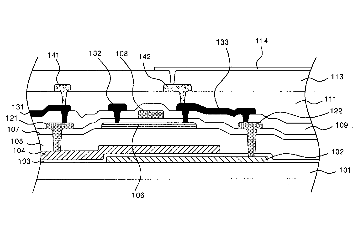
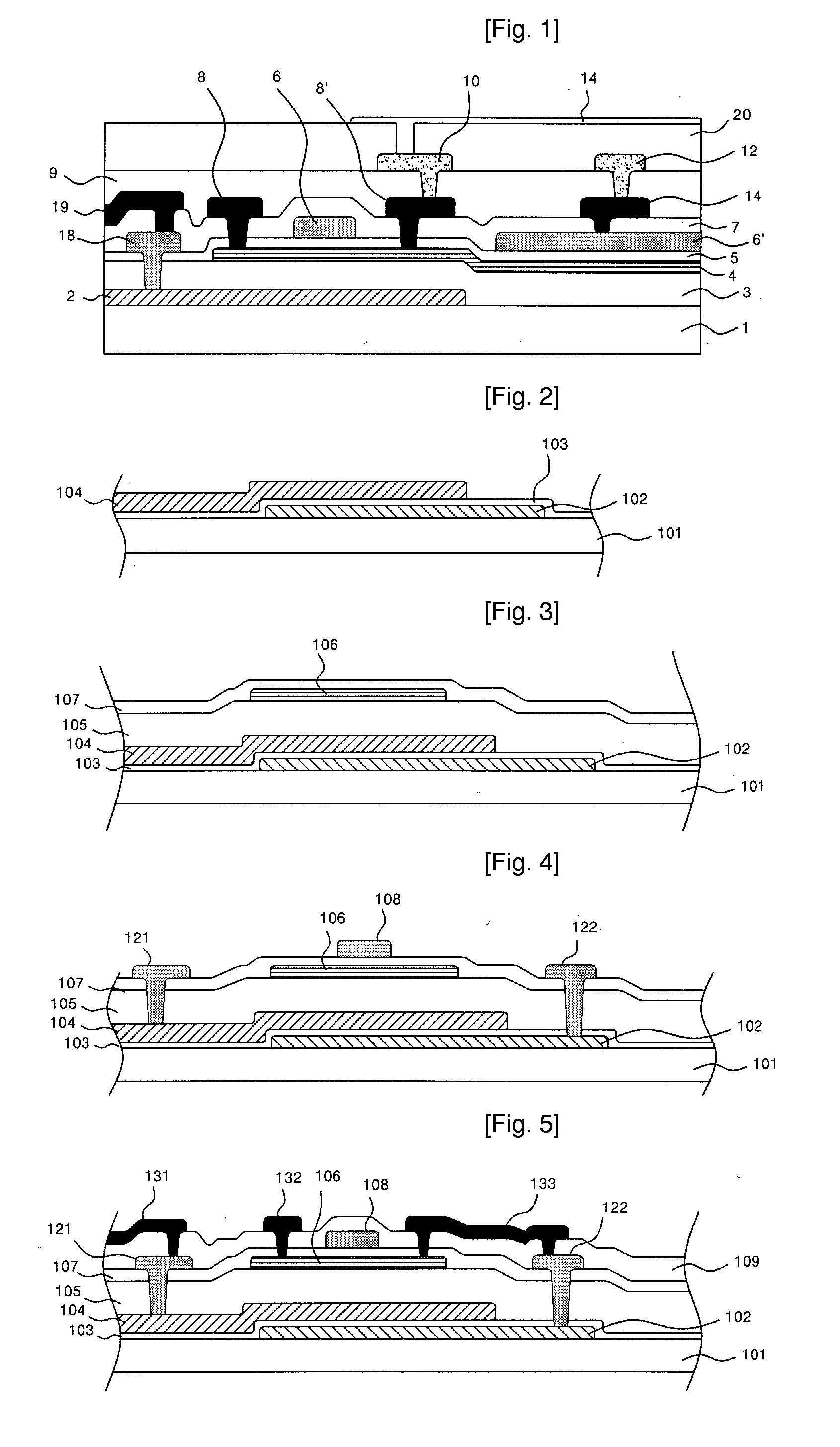
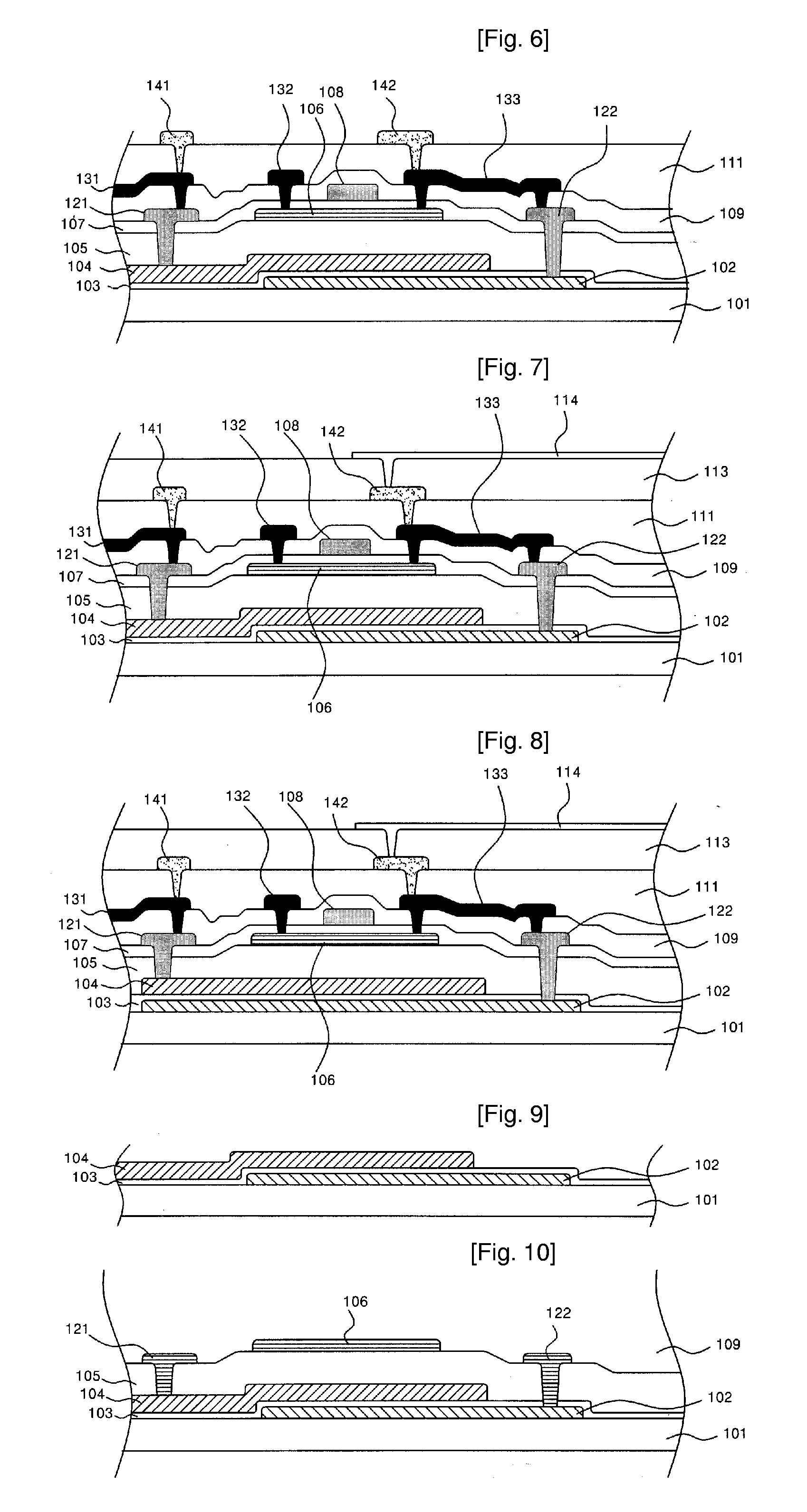
[0025]FIG. 2 to FIG. 7 are cut sectional views for illustrating a lower substrate manufacturing method of a thin film transistor in accordance with a desired embodiment of the present invention. A storage capacitor lower electrode (102) is formed by depositing and patterning a conductive film such as doped poly silicon or metal silicide on a transparent substrate (101). Next, a capacitor insulating film (103) is formed by depositing an insulating film through thermal oxidation or CVD (Chemical Vaporized Deposition), and a metal silicide film such as tungsten silicide (WSix) is deposited on the capacitor insulating film (103) while being patterned, functioning as a lower BM (Black Matrix) for cutting off a light incident on a channel unit of the thin film transistor and forming a storage capacitor upper electrode (104)(FIG. 2). Th...


PUM

PropertyMeasurementUnit
temperatureaaaaaaaaaa
transparentaaaaaaaaaa

Abstract

The present invention generally relates to a liquid crystal panel using a thin film transistor and a manufacturing method thereof, and more specifically to a liquid crystal panel using a thin film transistor and a manufacturing method thereof for improving an opening ratio by forming a storage capacitor under a channel. The present invention has suggested a method for effectively contacting an upper electrode for forming a capacitor with a lower electrode since the storage capacitor is located under the channel. Compared to a prior art in which one of storage capacitor electrodes is formed side by side with a channel of a thin film transistor, capacitor electrodes formed according to the present invention are located near to a substrate, thereby forming contact electrodes in many times without forming them one time.

Description

TECHNICAL FIELD [0001] The present invention relates to a liquid crystal display using a high-temperature poly silicon thin film transistor (TFT-LCD) used for a projection display device and a manufacturing method thereof, and more specifically to an LCD panel using a thin film transistor and a manufacturing method thereof for improving an opening ratio of a screen by minimizing an impermeable area of light, which is occupied by a storage capacitor. BACKGROUND ART [0002] Generally, while images are displayed on each pixel of an LCD panel using a thin film transistor for displaying with three primary colors such as R (red), G (green), and B (blue) colors, light leakage may occur among the pixels, influencing other pixels. As a result, sharpness may deteriorate. To solve the above problem, black matrices which cut off the light leakage while cutting off light to increase pixel sharpness are disposed among the pixels, thereby increasing sharpness of a screen. Besides, when light is inc...

Claims


Application Information

Patent Timeline
Patent Type & Authority Applications(United States)
IPC IPC(8): G02F1/136H01L21/00G02F1/1362
CPCG02F1/136209G02F2202/104G02F1/136227G02F1/136213B42F5/00B42F17/30G09B27/08G09B29/006
Inventor JANG, SEOK PILKIM, HONG RYUL
Owner ILJIN DISPLAY
Why Eureka
Try Eureka