Composite electrode for light-emitting device

a technology of light-emitting devices and composite electrodes, which is applied in the direction of semiconductor devices, basic electric elements, electrical apparatus, etc., can solve the problems of limiting the efficiency of oled devices, affecting the power distribution and manufacturability of light-emitting devices, and absorbing a large amount of light output from the light-emitting layer in the oled within the device, so as to achieve greater light-emission efficiency and improve power distribution and manufa

Active Publication Date: 2007-11-01
GLOBAL OLED TECH
View PDF18 Cites 39 Cited by
  • Summary
  • Abstract
  • Description
  • Claims
  • Application Information

AI Technical Summary

Benefits of technology

[0017] The present invention has the advantage that it provides electrodes that enable improved power distribution and manufacturability as well as greater light-emission efficiency in light emitting devices.

Problems solved by technology

However, as is well known, much of the light output from the light-emissive layer in the OLED is absorbed within the device.
In general, up to 80% of the light may be lost in this manner.
It has been found, however, that one of the key factors that limits the efficiency of OLED devices is the inefficiency in extracting the photons generated by the electron-hole recombination out of the OLED devices.
Due to the high optical indices of the organic materials used, most of the photons generated by the recombination process are actually trapped in the devices due to total internal reflection.
The particular arrangement, however, has difficulty in providing an adequate supply of current to all areas of an OLED, since it relies upon a transparent electrode for the distribution of power and it is known that transparent electrodes suffer from inadequate conductivity.
However, many electrode materials that are transparent, such as ITO, have relatively low conductivity, which may result in a voltage drop across the display.
This in turn may cause variable light output from the light emitting elements in the display, resistive heating, and power loss.
However, the deposition of the auxiliary electrode typically requires expensive patterning processes.
Since scattering layers typically include particles with sharp edges, electrical shorts between the electrodes often result, making the OLED inoperative.

Method used


Image

  • Composite electrode for light-emitting device
  • Composite electrode for light-emitting device
  • Composite electrode for light-emitting device

Examples


Embodiment Construction

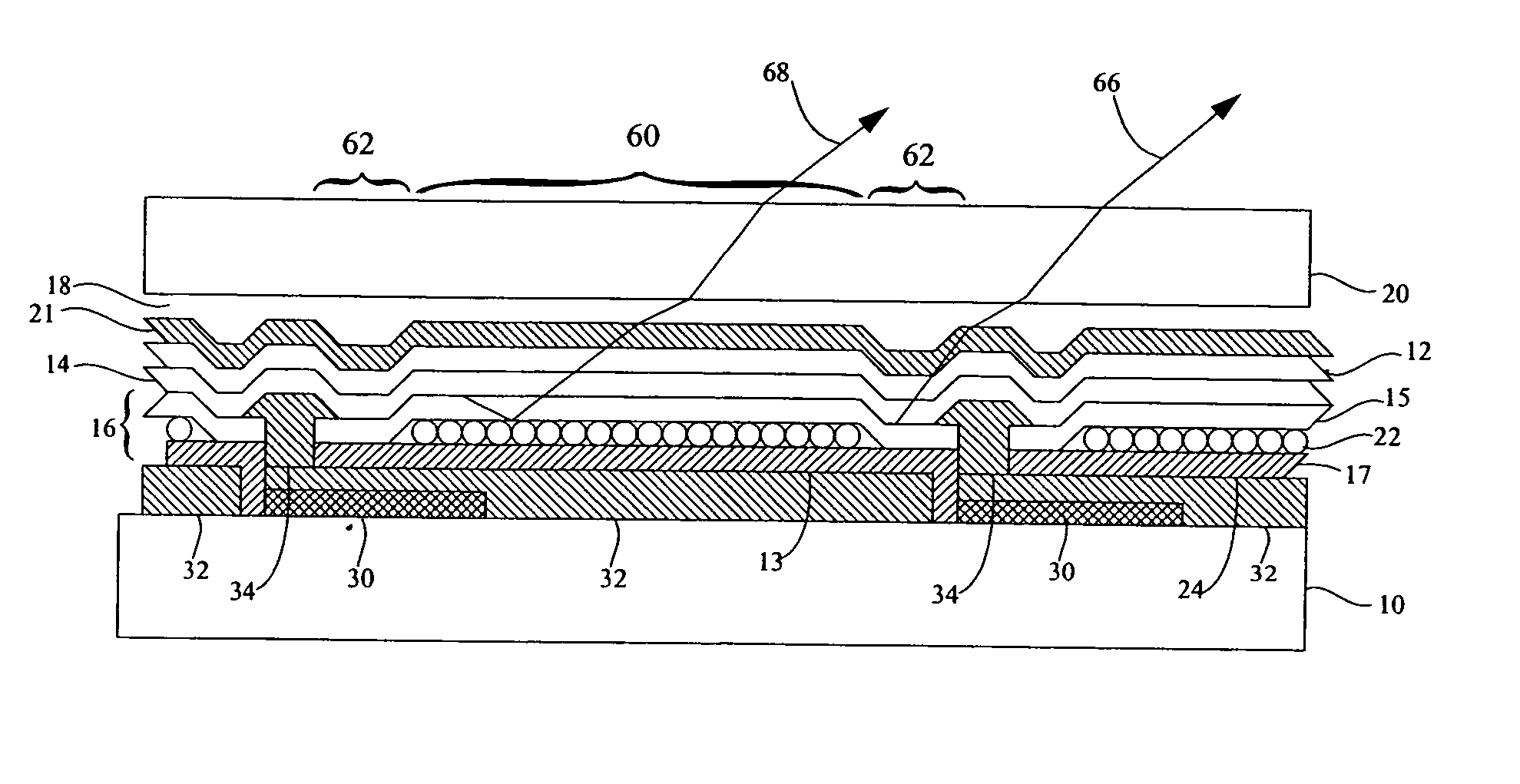
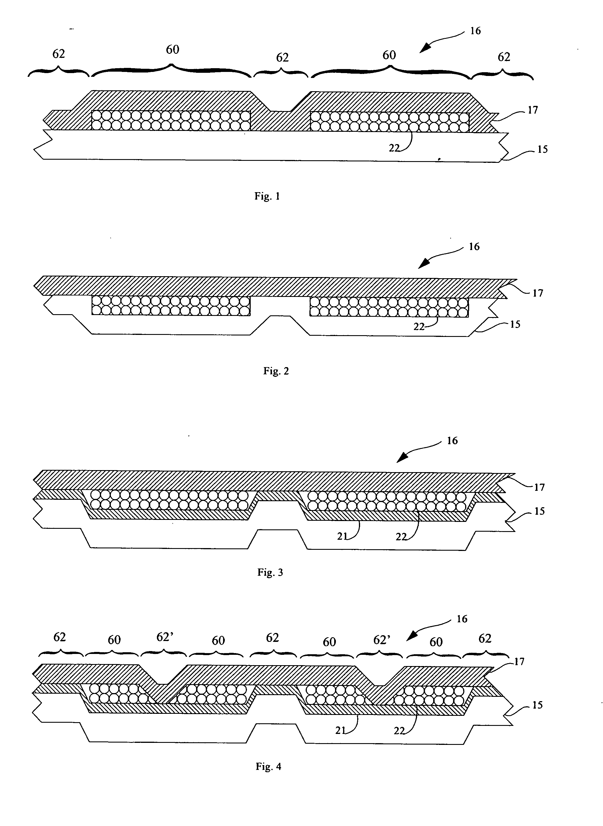
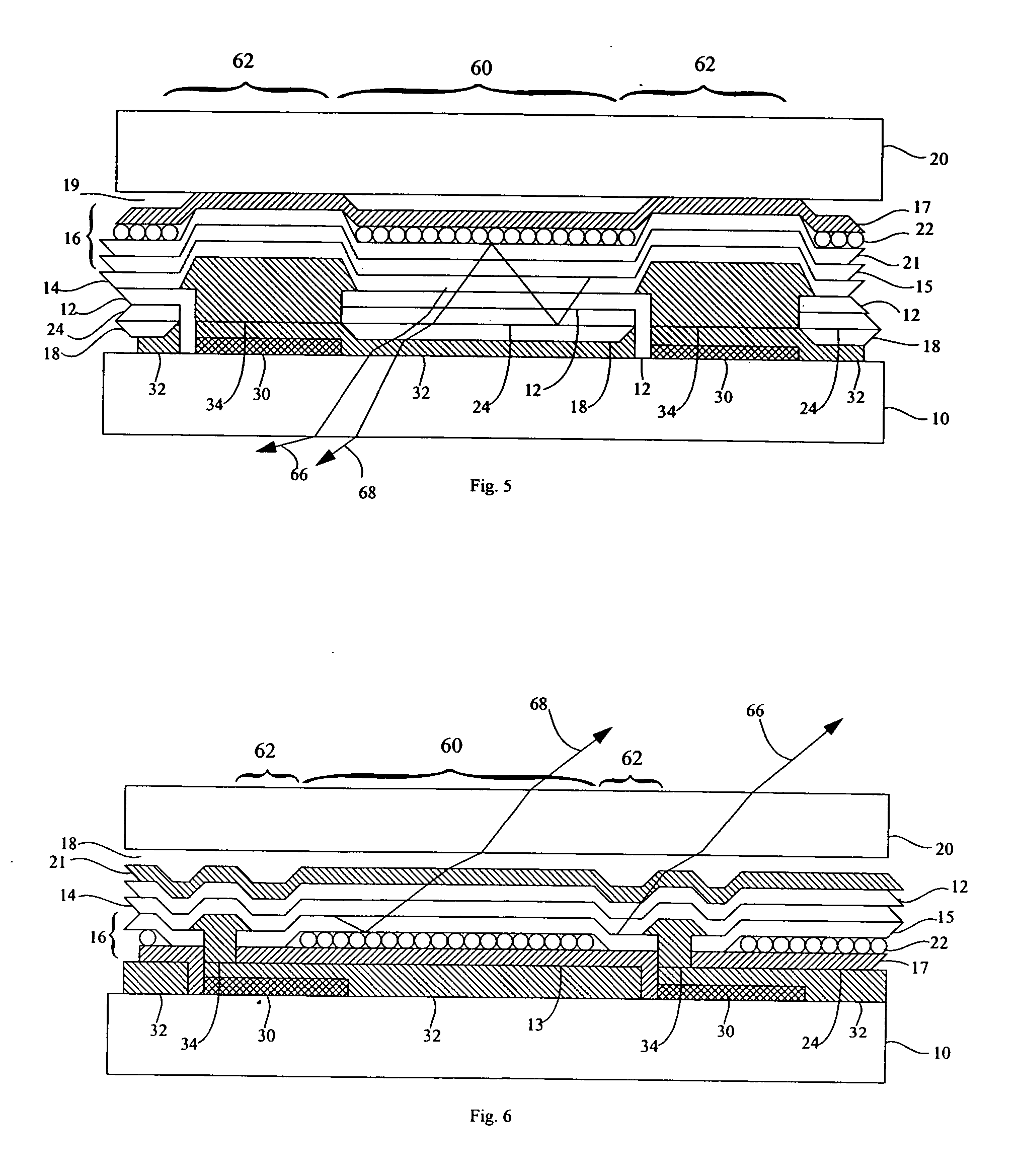
[0026] Referring to FIG. 1, in accordance with one embodiment of the present invention, a multi-layer composite electrode 16 for an OLED device comprises a transparent, conductive layer 15 and a reflective, conductive layer 17 in electrical contact with the transparent, conductive layer 15. A light-scattering layer 22 is formed between the transparent, conductive layer 15 and the reflective, conductive layer 17 over only first portion 60 of the transparent, conductive layer 15. Light-scattering layer 22 is relatively less conductive than the reflective, conductive layer 17 and the reflective, conductive layer 17 is in electrical contact with the transparent, conductive layer 15 over second portion 62 of the transparent, conductive layer 15 where the light-scattering layer 22 is not formed. In various embodiments, the scattering layer 22 may comprise transparent refractive particles, reflective particles, and / or conductive particles.

[0027] In various embodiments of the present inven...


PUM

PropertyMeasurementUnit
thicknessaaaaaaaaaa
thickaaaaaaaaaa
thickaaaaaaaaaa

Abstract

A multi-layer composite electrode for a light-emitting device, comprising: a transparent, conductive layer; a reflective, conductive layer in electrical contact with the transparent, conductive layer; and a light-scattering layer formed between the transparent, conductive layer and the reflective, conductive layer over only a first portion of the transparent, conductive layer, wherein the light-scattering layer is relatively less conductive than the reflective, conductive layer and the reflective, conductive layer is in electrical contact with the transparent, conductive layer over a second portion of the transparent, conductive layer where the light-scattering layer is not formed. Also disclosed is a method of making such a multi-layer composite electrode in a light emitting device, and an organic light-emitting diode (OLED) device comprising such a composite electrode.

Description

FIELD OF THE INVENTION [0001] The present invention relates to electrodes for light-emitting devices, and more particularly to composite electrodes comprising a light scattering layer for organic light-emitting diode (OLED) devices for improving light output. BACKGROUND OF THE INVENTION [0002] Organic light-emitting diodes (OLEDs) are a promising technology for flat-panel displays and area illumination lamps. The technology relies upon thin-film layers of materials coated upon a substrate. However, as is well known, much of the light output from the light-emissive layer in the OLED is absorbed within the device. Because light is emitted in all directions from the internal layers of the OLED, some of the light is emitted directly from the device, and some is emitted into the device and is either reflected back out or is absorbed, and some of the light is emitted laterally and trapped and absorbed by the various layers comprising the device. In general, up to 80% of the light may be l...

Claims


Application Information

Patent Timeline
Patent Type & Authority Applications(United States)
IPC IPC(8): H01L33/00H01L31/12H01L27/15H01L29/26
CPCH01L51/5268H01L51/5203H10K50/805H10K50/854
Inventor COK, RONALD S.
Owner GLOBAL OLED TECH
Why Eureka
Try Eureka