Structure of electronic package and printed circuit board thereof
- Summary
- Abstract
- Description
- Claims
- Application Information
AI Technical Summary
Benefits of technology
Problems solved by technology
Method used
Image

Examples
Embodiment Construction
[0017] The embodiments of the present invention are illustrated in reference to the drawings.
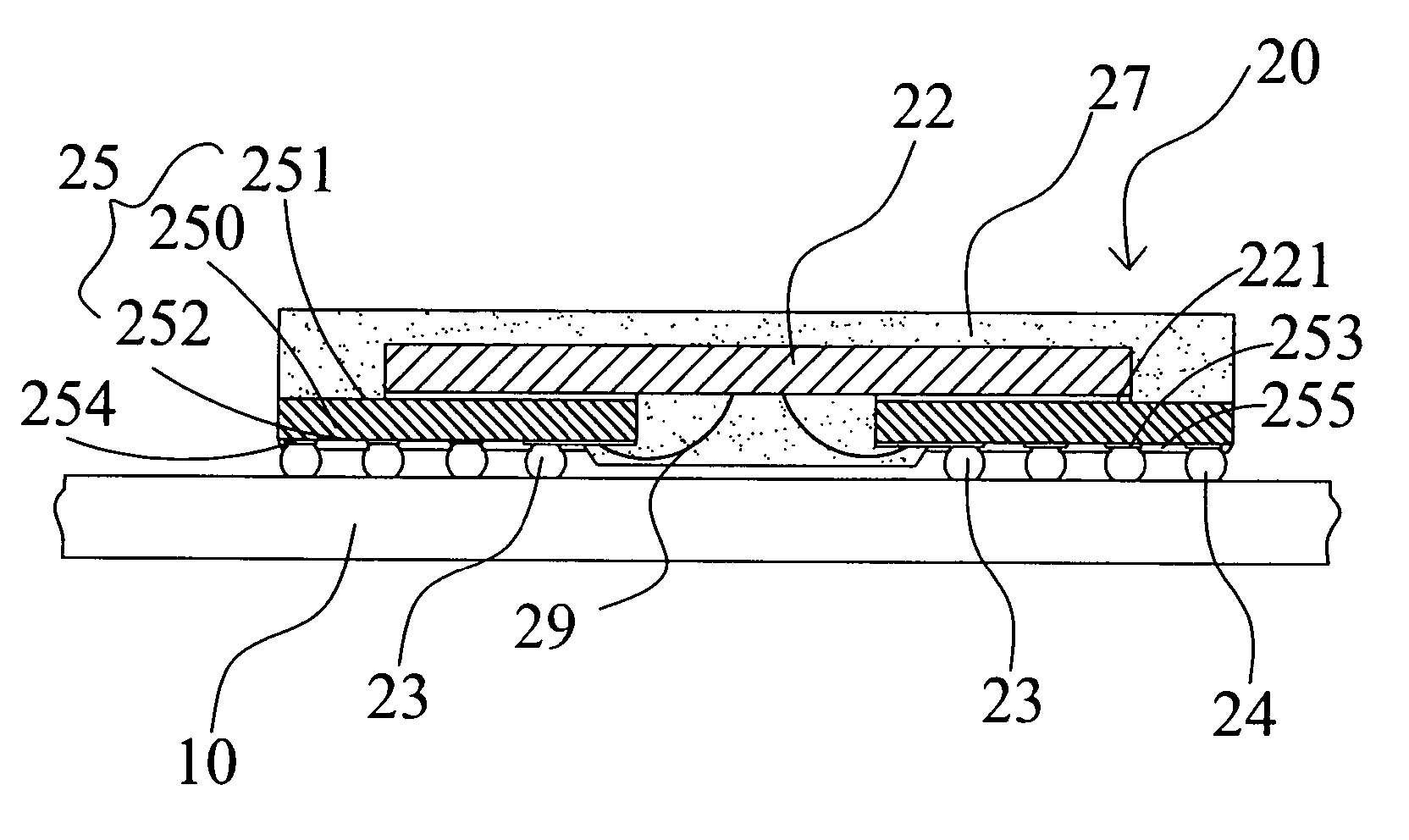
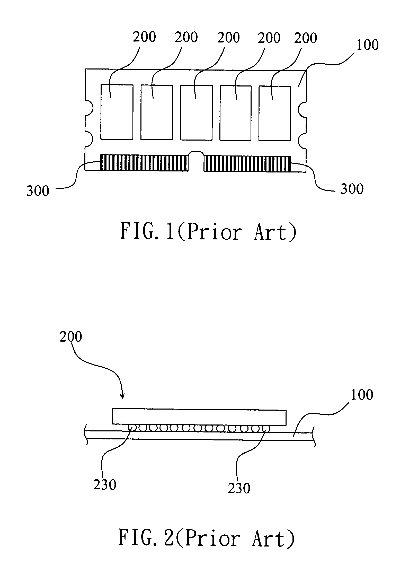
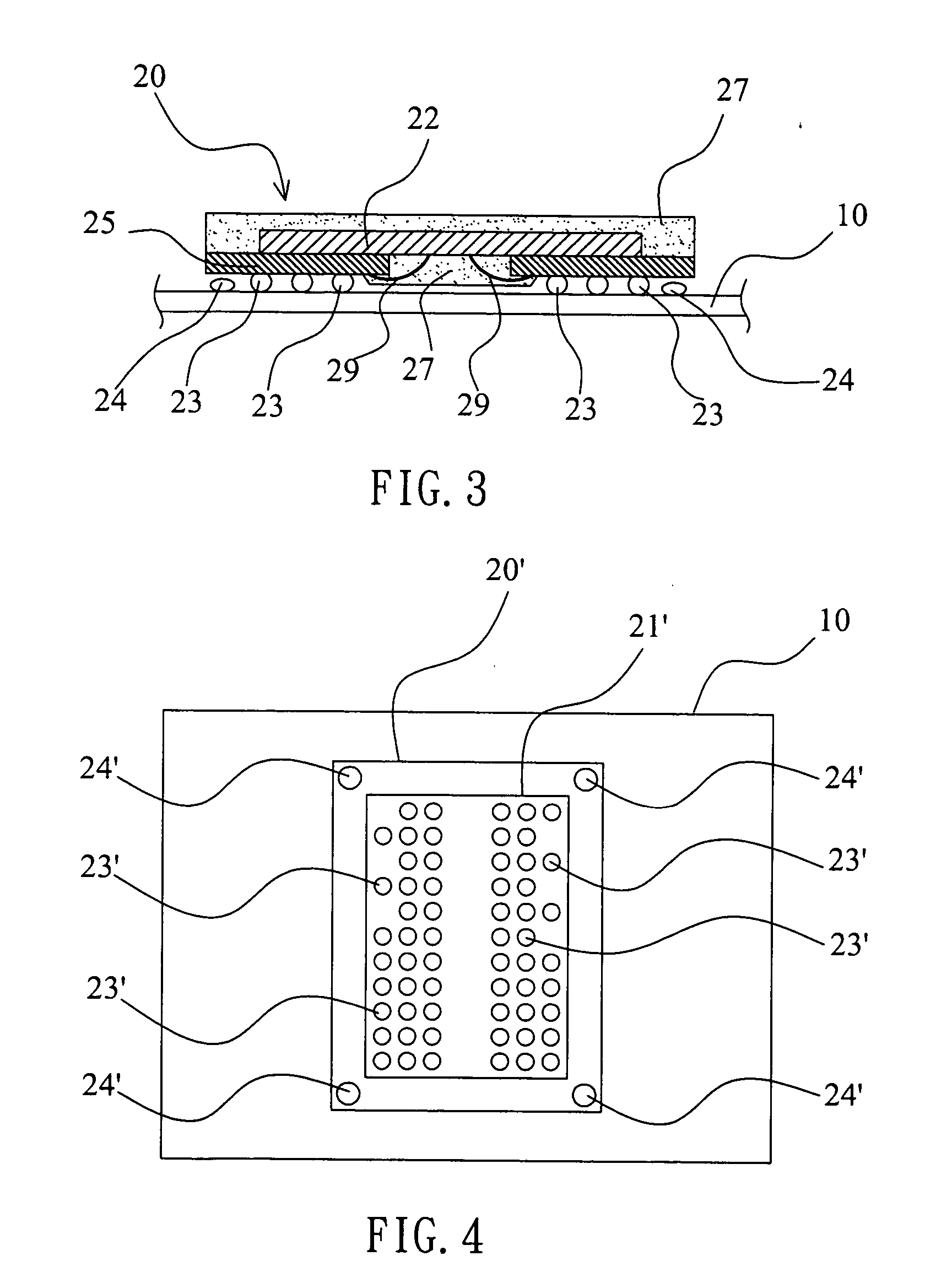
[0018]FIG. 3 is a portion of side-view schematic diagram illustrating a package of IC assembled on a printed circuit board (PCB). Shown in FIG. 3, an exterior element, such as a package of IC 20 is assembled on one surface of a printed circuit board (PCB) 10. In the embodiment, the package of IC 20 is a window BGA, but not limited to.
[0019] Next, a chip 22 is fixed or attached on one surface of a substrate 25 with a die-attached material (not shown). In the embodiment, the substrate 25 is with a window path which a plurality of structures of conductive connection 29 are electrically connected the chip 22 and the substrate 25. A molding compound 27 covers the chip 22 and the structures of conductive connection 29 to make the package of IC 20. The package of IC 20 may include a plurality of conductive balls 23 that are attached to and electrically connected to the printed circuit board 10. A...
PUM
 Abstract
Description
Claims
Application Information
 - Generate Ideas
- Intellectual Property
- Life Sciences
- Materials
- Tech Scout
- Unparalleled Data Quality
- Higher Quality Content
- 60% Fewer Hallucinations
Browse by: Latest US Patents, China's latest patents, Technical Efficacy Thesaurus, Application Domain, Technology Topic, Popular Technical Reports.
© 2025 PatSnap. All rights reserved.Legal|Privacy policy|Modern Slavery Act Transparency Statement|Sitemap|About US| Contact US: help@patsnap.com