Semiconductor integrated circuit, manufacturing method thereof, and semiconductor device using semiconductor integrated circuit

a semiconductor integrated circuit and integrated circuit technology, applied in the direction of semiconductor devices, semiconductor/solid-state device details, electrical apparatus, etc., can solve the problems of long time, reduced productivity, and defect in the integrated circuit, so as to prevent contamination of the semiconductor integrated circuit, suppress the generation of dust, and improve the effect of productivity

Inactive Publication Date: 2007-11-01
SEMICON ENERGY LAB CO LTD
View PDF8 Cites 68 Cited by
  • Summary
  • Abstract
  • Description
  • Claims
  • Application Information

AI Technical Summary

Benefits of technology

[0007]It is an object of the present invention to improve the productivity of an integrated circuit which is formed by stacking semiconductors. It is another object of the present invention to provide a method for manufacturing a semiconductor integrated circuit having mechanical flexibility by thinning an integrated circuit which is formed by stacking semiconductors.
[0016]Note that a release layer in this specification means a layer which makes it easy to peel off a plurality of layers having semiconductor elements from a substrate.
[0017]In the present invention, when an integrated circuit including a semiconductor element which is formed using a semiconductor layer and insulating layers sandwiching the semiconductor layer is formed over a substrate, and peeled off from the substrate, and then stacked, an integrated circuit which is formed by stacking semiconductors can be thinned. In addition, by forming a semiconductor integrated circuit of the present invention over a flexible substrate such as plastic, a semiconductor device which is thin, lightweight, and flexible can be formed.
[0018]In addition, since a step of forming a through hole in a semiconductor substrate having a thickness of several micrometers to several hundred micrometers is omitted, productivity can be improved. That is, since the semiconductor substrate is not required to be polished so as to form a through hole in the semiconductor substrate, generation of dust can be suppressed, and contamination of a semiconductor integrated circuit can be prevented.

Problems solved by technology

In this manner, a step of forming a through hole in a semiconductor substrate, or a step of polishing the semiconductor substrate from its back surface requires a very long time and causes decrease of productivity.
In addition, in a step of forming a through hole in the semiconductor substrate or a step of polishing the semiconductor substrate from its back surface, dust is generated, which causes a defect in an integrated circuit.
In addition, a semiconductor integrated circuit which is formed by stacking semiconductors has a structure in which semiconductor substrates are stacked; therefore, the semiconductor integrated circuit has a thick structure and poor mechanical flexibility.

Method used


Image

  • Semiconductor integrated circuit, manufacturing method thereof, and semiconductor device using semiconductor integrated circuit
  • Semiconductor integrated circuit, manufacturing method thereof, and semiconductor device using semiconductor integrated circuit
  • Semiconductor integrated circuit, manufacturing method thereof, and semiconductor device using semiconductor integrated circuit

Examples


embodiment mode 1

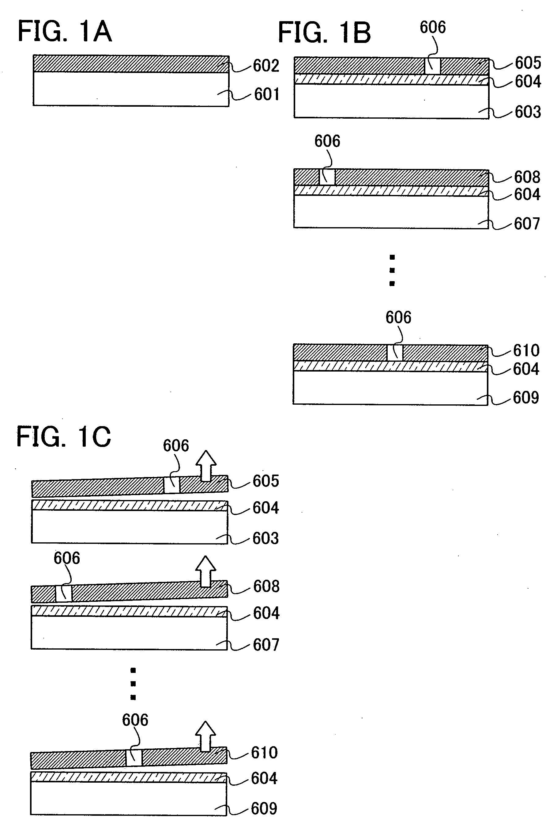
[0053]A semiconductor integrated circuit of this embodiment mode is provided with a layer (hereinafter also referred to as an element formation layer) having semiconductor elements, which is formed over each of a plurality of substrates. When the layer having the semiconductor elements is peeled off, and then, overlapped and attached to another substrate, the semiconductor integrated circuit of this embodiment mode is formed. In order to peel off the layer having the semiconductor elements from the substrate, a release layer is formed over the substrate, and the layer having the semiconductor elements is formed over the release layer. In addition, the layer having the semiconductor elements, which is overlapped and attached to each other, is electrically connected to an upper layer or a lower layer with a through wiring.

[0054]This embodiment mode will briefly describe a method for forming a semiconductor integrated circuit of the present invention with reference to FIGS. 1A to 3D.

[0...

embodiment mode 2

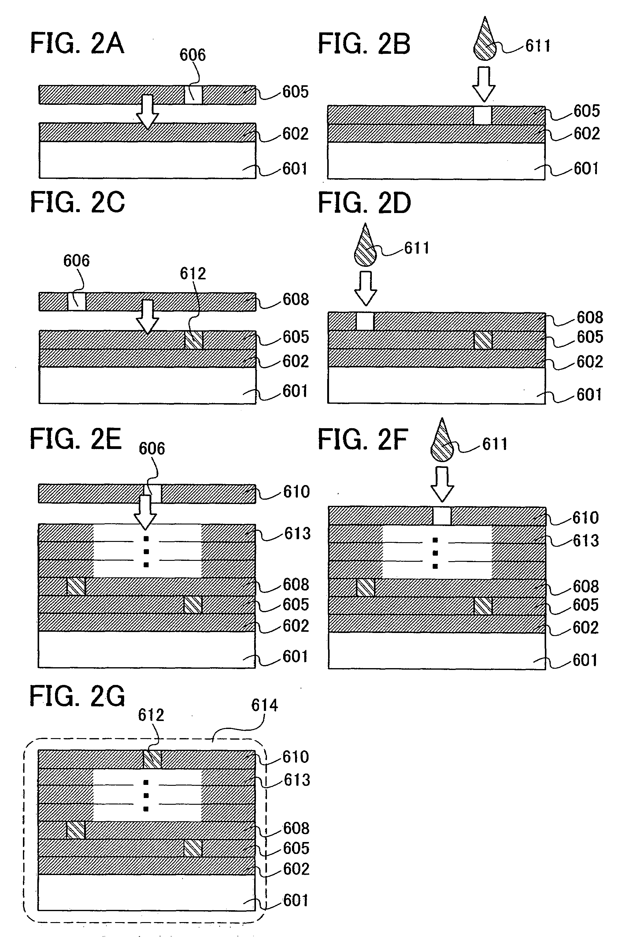
[0080]This embodiment mode will describe a method for forming the first to n-th element formation layers which form the semiconductor integrated circuit described in Embodiment Mode 1, and a method for forming a semiconductor integrated circuit by stacking those element formation layers, with reference to FIGS. 4A to 10B. Here, FIGS. 4A to 9B show cross-sectional views of a substrate, and FIGS. 10A and 10B show top views of a substrate.

[0081]First, a method for manufacturing the second to n-th element formation layers in Embodiment Mode 1 will be described. First, a first insulating layer 101 is formed over one surface of a substrate 100. Next, a release layer 102 is formed over the first insulating layer 101. Then, a second insulating layer 103 is formed over the release layer 102 (see FIG. 4A).

[0082]The substrate 100 is a substrate having an insulating surface, for example, a glass substrate, a quartz substrate, a resin (plastic) substrate, a sapphire substrate, a silicon wafer or...

embodiment mode 3

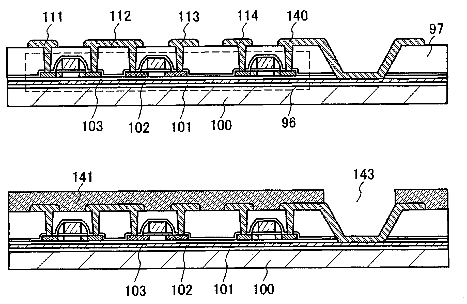
[0138]This embodiment mode will describe a method for forming a semiconductor integrated circuit which has a different structure from Embodiment Mode 2, with reference to drawings. This embodiment mode differs from Embodiment Mode 2, in that, when the first element formation layer to the n-th element formation layer are stacked, a conductive material is sandwiched between the element formation layers.

[0139]FIGS. 11A to 11C show cross-sectional views of the first element formation layer to the n-th element formation layer for forming a semiconductor integrated circuit. Since steps up to and including the formation of the second conductive layers 111 to 116 are the same as the steps up to and including the stage shown in FIG. 4D of Embodiment Mode 2, description thereof is omitted here. A fifth insulating layer 150 is selectively formed so as to cover the fourth insulating layers 97 and the second conductive layers 111 to 116 (see FIG. 11A). The fifth insulating layer 150 is not forme...


PUM


Abstract

A step of forming a through hole in a semiconductor substrate, or a step of polishing the semiconductor substrate from its back surface requires a very long time and causes decrease of productivity. In addition, when semiconductor substrates are stacked, a semiconductor integrated circuit which is formed of the stack is thick and has poor mechanical flexibility. A release layer is formed over each of a plurality of substrates, layers each having a semiconductor element and an opening for forming a through wiring are formed over each of the release layers. Then, layers each having the semiconductor element are peeled off from the substrates, and then overlapped and stacked, a conductive layer is formed in the opening, and the through wiring is formed; thus, a semiconductor integrated circuit is formed.

Description

BACKGROUND OF THE INVENTION[0001]1. Field of the Invention[0002]The present invention relates to a semiconductor integrated circuit which is formed by stacking semiconductor elements.[0003]2. Description of the Related Art[0004]A technique for highly integrating a semiconductor integrated circuit has been developed by stacking semiconductor substrates provided with integrated circuits. Such a semiconductor integrated circuit which is formed by stacking semiconductors has been manufactured by sequentially stacking semiconductor substrates provided with integrated circuits. The semiconductor integrated circuit which is formed by stacking the semiconductors is formed such that semiconductor substrates are each provided with an integrated circuit and stacked by thinning the semiconductor substrates or the like (see e.g., Reference 1: Japanese Published Patent Application No. H6-61418, and Reference 2: Japanese Published Patent Application No. 2001-189419).SUMMARY OF THE INVENTION[0005]H...

Claims


Application Information

Patent Timeline
Patent Type & Authority Applications(United States)
IPC IPC(8): H01L21/30H01L21/46
CPCH01L21/6835H01L21/8221H01L2924/07811H01L2924/1305H01L2924/12032H01L27/124H01L2924/13091H01L2924/01019H01L2924/12044H01L21/84H01L23/4985H01L23/49855H01L23/5389H01L25/105H01L27/0688H01L27/12H01L27/1266H01L2224/24145H01L2224/76155H01L2924/00H01L21/76879H01L21/288
Inventor YAMAGUCHI, MAYUMIIZUMI, KONAMI
Owner SEMICON ENERGY LAB CO LTD
Why Eureka
Try Eureka