Programmable asynchronous first-in-first-out (FIFO) structure with merging capability

a first-in-first-out, asynchronous technology, applied in the field of high-speed data communication, can solve the problems of significant challenge in meeting a low-latency objective, host performance in memory access latency may be significantly affected, and achieve the effect of improving latency and power consumption of high-speed circuitry

Active Publication Date: 2007-11-08
RAMBUS INC
View PDF4 Cites 27 Cited by
  • Summary
  • Abstract
  • Description
  • Claims
  • Application Information

AI Technical Summary

Benefits of technology

[0018]It is therefore an objective of the present invention to develop a circuitry and a method for constructing an asynchronous FIFO with merging capability that significantly improves latency while at the same time permits keeping the power consumption of the high speed circuitry as low as possible.

Problems solved by technology

In addition jitter and wander occurs.
This architecture which employs serial links (requiring serial / parallel conversions) and the daisy chaining of the links through the AMBs 122 containing dejitterizing circuits with inherent delay, presents a significant challenge in meeting a low-latency objective.
Even though the links run at very high speed, host performance in terms of memory access latency may be significantly affected by the round trip delay imposed on a read operation, caused by the latency imposed by the AMB circuitry.

Method used


Image

  • Programmable asynchronous first-in-first-out (FIFO) structure with merging capability
  • Programmable asynchronous first-in-first-out (FIFO) structure with merging capability
  • Programmable asynchronous first-in-first-out (FIFO) structure with merging capability

Examples


Embodiment Construction

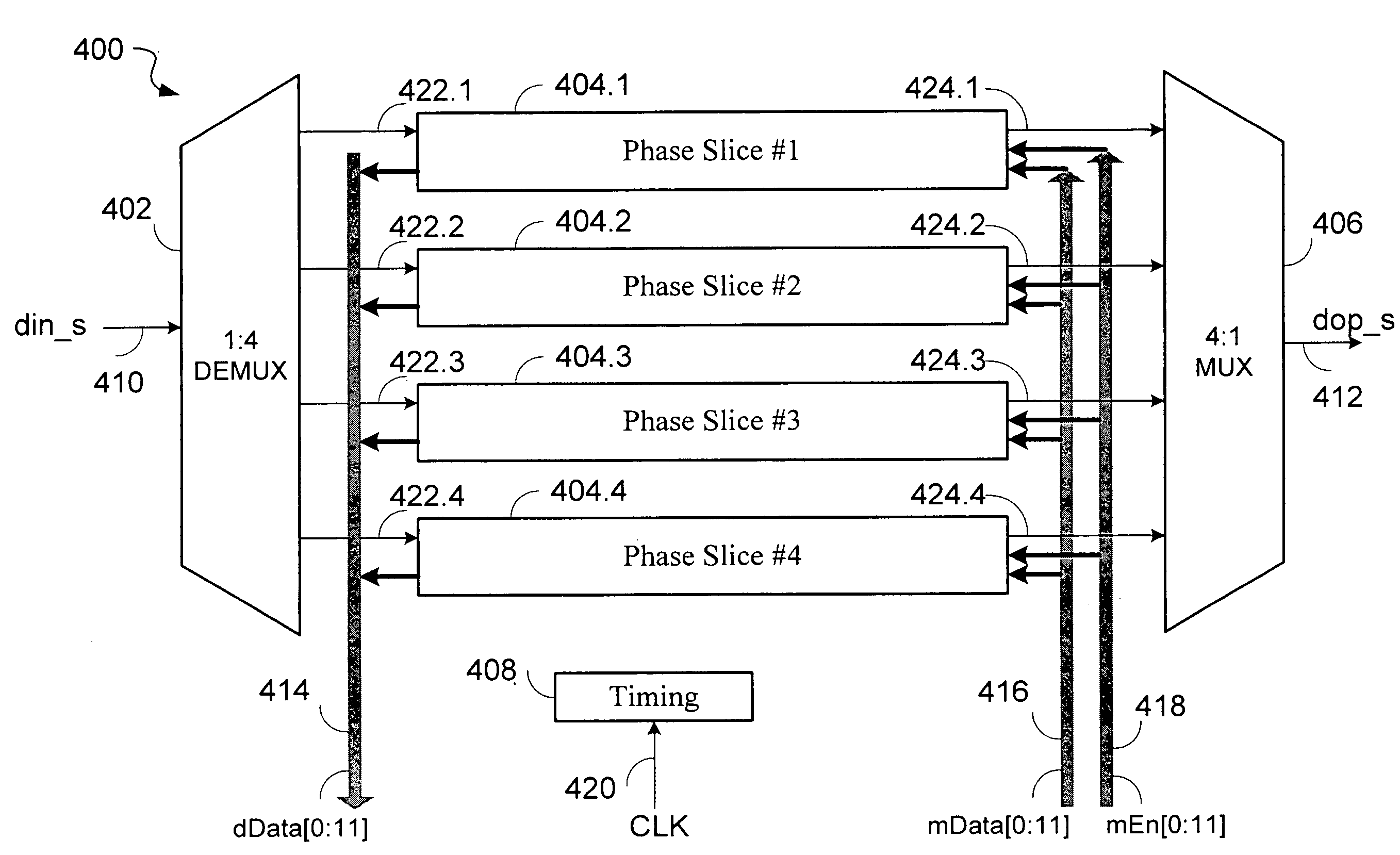
[0115]FIG. 2 shows a block diagram of a typical Advanced Memory Buffer (AMB) 200 according to an embodiment of the invention. An AMB according to the afore-mentioned JEDEC specification may provide buffering for up to ten upstream channels 124 and up to fourteen downstream channels 126 (see FIG. 1). Accordingly, the AMB 200 includes twenty-four (10+14) buffer circuits termed “Channel Slice #1” to “Channel Slice #24” (202 typ), and a “Core”204. The buffer functionality required in the downstream channels 126 is a subset of the buffer functionality required in the upstream channels 124, and a single design for all twenty-four Channel Slices 202 is presented here.

[0116]The Channel Slices 202 of the AMB 200 include innovative data buffering circuitry and individual timing circuitry “Channel Timing”206.

[0117]The Core 204 of the AMB 200 includes common control functions and interfaces to the DRAMs 120 that are located on the subject FBD. The Core 204 further includes common clock circuitr...


PUM


Abstract

Where high speed communication between a host and memory devices is carried over serial bit lanes, memory buffers are required for converting buffering the serial bit lanes, and for converting between serial and parallel formats. In addition, jitter, wander, and skew between the bit lanes need to be accommodated. The invention discloses a programmable asynchronous FIFO with the integrated ability to convert blocks of bits from serial to parallel as well as inserting bits from a parallel bus into the serial bit stream. The invention provides very low latency and can be implemented in low power technologies.

Description

FIELD OF THE INVENTION[0001]The present invention relates generally to data processing systems and more particularly to high-speed data communication between hosts and memory subsystems.BACKGROUND OF THE INVENTION[0002]A number of architectures are available for interconnecting processors with memory devices. As a simple example, a processor may be directly connected with memory devices over a conventional memory bus. In modem high performance computer systems, memory may accessed through a memory controller, and the memory devices may be mounted on sub-assemblies (Dual In-line Memory Modules, or DIMMs) which themselves include a memory buffer in addition to the individual memory devices.[0003]One such architecture is described in detail in a proposed JEDEC (Joint Electrical Device Engineering Council) Standard entitled FB-DIMM Draft Specification, jointly published in March 2005 by the JEDEC Solid State Technology Association, and EIA (Electrical Industries Alliance).[0004]In this ...

Claims


Application Information

Patent Timeline
Patent Type & Authority Applications(United States)
IPC IPC(8): H04J3/04
CPCH04L7/033
Inventor REITLINGSHOEFER, CLAUSPFAFF, DIRKBADALONE, RICCARDO
Owner RAMBUS INC
Why Eureka
Try Eureka