Semiconductor light emitting device and a method for producing the same

a technology of light-emitting devices and semiconductors, which is applied in the direction of semiconductor devices, basic electric elements, electrical appliances, etc., can solve the problems of reduced resistance of lead terminal portions, prone to oxidation to rust, and thick led light-emitting devices, so as to reduce the possibility of damage to them, prevent damage, and less prone to damage

Active Publication Date: 2007-11-15
NICHIA CORP
View PDF4 Cites 186 Cited by
  • Summary
  • Abstract
  • Description
  • Claims
  • Application Information

AI Technical Summary

Benefits of technology

[0024]According to the semiconductor light emitting device in the first or tenth aspect of the present invention, the lead terminal smaller projection(s) is / are located between the pair of outer lead projections, and additionally the end surface(s) of the lead smaller projection(s) is adjusted whereby projecting less than the end surfaces of the outer lead projections. Thus, the lead terminal smaller projection(s) does / do not project outward of the outer lead projections. For this reason, even in the case where corners of the lead terminal smaller projection(s) are not rounded, the lead terminal smaller projection(s) can be less prone to damage to other members due to edged corners. Therefore, in mass-production processes of a number of semiconductor light emitting devices, it is possible to prevent damage even if the semiconductor light emitting devices come in contact with each other. In addition, according to the semiconductor light emitting device in the second aspect of the present invention, the corners of the outer lead projections are rounded, thus, even if these parts come in contact with other members, it is possible to reduce possibility of damage to them. In addition, according to the semiconductor light emitting device in the third aspect of the present invention, since the lead terminal smaller projection(s) does / do not project, even in the case where the corners of the lead terminal smaller projection(s) are not rounded but are edged, these parts can be less prone to cause damage. Therefore it is possible to save time and effort of processing the lead terminal smaller projection(s).
[0025]In addition, according to the semiconductor light emitting device in the fourth aspect of the present invention, since two lead terminal smaller projections are formed in each outer lead region, in production processes, the lead arrangement can be stably held. Additionally, each of the two lead terminal smaller projections is located between the middle outer lead projection and each of the end side outer lead projections, thus, even after production, these lead terminal smaller projections can be less prone to project outward of the outer lead regions. In addition, according to the semiconductor light emitting device in the fifth aspect of the present invention, a plurality of the outer lead projections have end surfaces that are substantially coplanar with each other, and a plurality of the lead terminal smaller projections have end surfaces that are substantially coplanar with each other, thus, this construction can provide an advantage in installation of the semiconductor light emitting device. In addition, according to the semiconductor light emitting device in the sixth aspect of the present invention, the protection film protects the lead arrangement, therefore, it is possible to prevent oxidation or the like. In the case where the lead terminal smaller projection is not protected by the protection film, this may cause poor adhesiveness due to corrosion. However, according to the semiconductor light emitting device in the seventh aspect of the present invention, since the end portion of the outer lead projection that is protected by the protection film has a large area, it is possible to maintain wettability of solder in installation, or the like, and thus to improve installation strength. As a result, it is possible to improve reliability. Therefore, it is possible to avoid problems due to exposure of side surfaces of the lead terminal smaller projection on which a protection film does not cover.
[0026]In addition, according to the semiconductor light emitting device in the eighth aspect of the present invention, the lead arrangement embedded in the package has a bent structure, thus, it is possible to improve engagement when the package is secured. Therefore, it is possible to improve adhesiveness.
[0027]In addition, according to the semiconductor light emitting device in the ninth aspect of the present invention, the bottom surface of the lead middle region is externally exposed, and is coplanar with the outer lead region, thus, the bottom surface of the lead middle region can be used as a terminal. Additionally, in the case where this part is coupled to a member with excellent thermal conductivity, it is possible to directly and outwardly dissipate heat generated by the light emitting element mounted on the lead middle region through the lead middle region.
[0028]Still furthermore, according to the semiconductor light emitting device in the eleventh aspect of the present invention, since a die-bonding material is diffused in a location where that provides electrical connection for the protection element on the lead arrangement, it is possible to prevent poor electrical conduction.

Problems solved by technology

This installation provides electrically connection between the LED chip 203 and the mount body 201 through the lead terminal portion 205a. However, in this construction, there are problems that require a process for bending the lead terminal portion so as to adjust its alignment along the side and bottom surfaces of the semiconductor light emitting device, reduce resistance of lead terminal portion due to the bent lead terminal portion, and make the LED light emitting device thick since the lead terminal portion is bent so as to extend the side and bottom surfaces thereof.
For this reason, this cut surface is prone to be oxidized to rust.
Additionally, since the oxidized cut surface 205c has poor wettability, solder or the like crawls.
As a result, there is a problem that causes insufficient adhesiveness between the oxidized cut surface 205c and the mount body 201.
Additionally, in mass-production processes of a number of LED light emitting devices, the sharp cut surface 205c of the lead terminal portion that projects from the end surface of one LED light emitting device may damage other semiconductor light emitting devices.
Additionally, long lead terminal portions reduce the number of leads that are arranged in patterns in one sheet of lead frame, and thus cause poor efficiency and comparatively high cost.
As a result, there is a problem that the reach of light emitted from the LED light emitting device 200 is deviated.
In addition, the lead terminal portion 205a may not completely align along the bottom surface of the package 206, as a result, there is a problem that the LED light emitting device 200 and the mount body 201 are not stably and mechanically or electrically coupled to each other.
This increases the defect due to the aforementioned cut surface of the lead terminal portion.
Since this projection portion has edged corners, these parts may damage other light emitting devices 300.
On the other hand, the defect that the cut surface is oxidized in air is not still solved.

Method used


Image

  • Semiconductor light emitting device and a method for producing the same
  • Semiconductor light emitting device and a method for producing the same
  • Semiconductor light emitting device and a method for producing the same

Examples


first embodiment

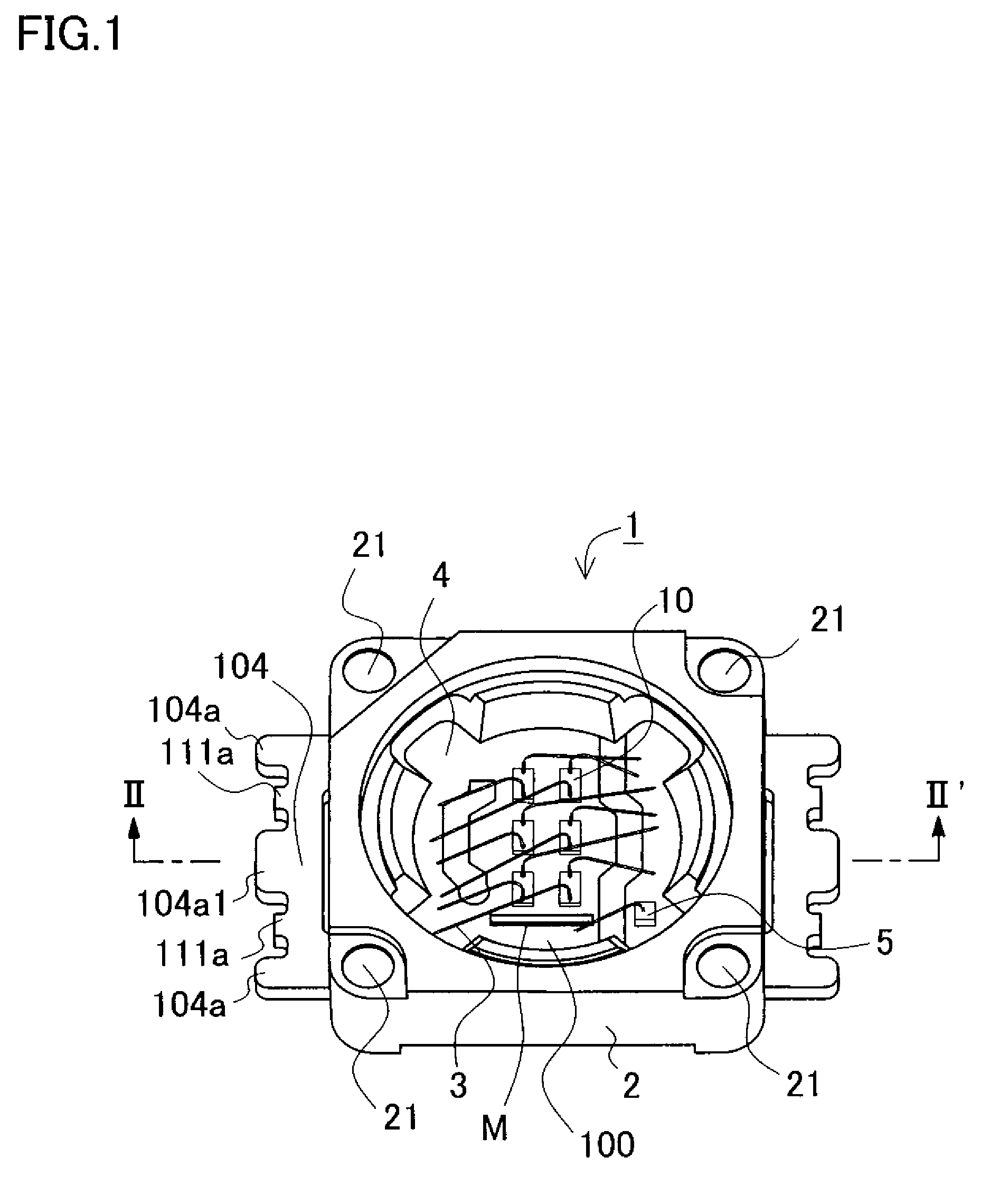
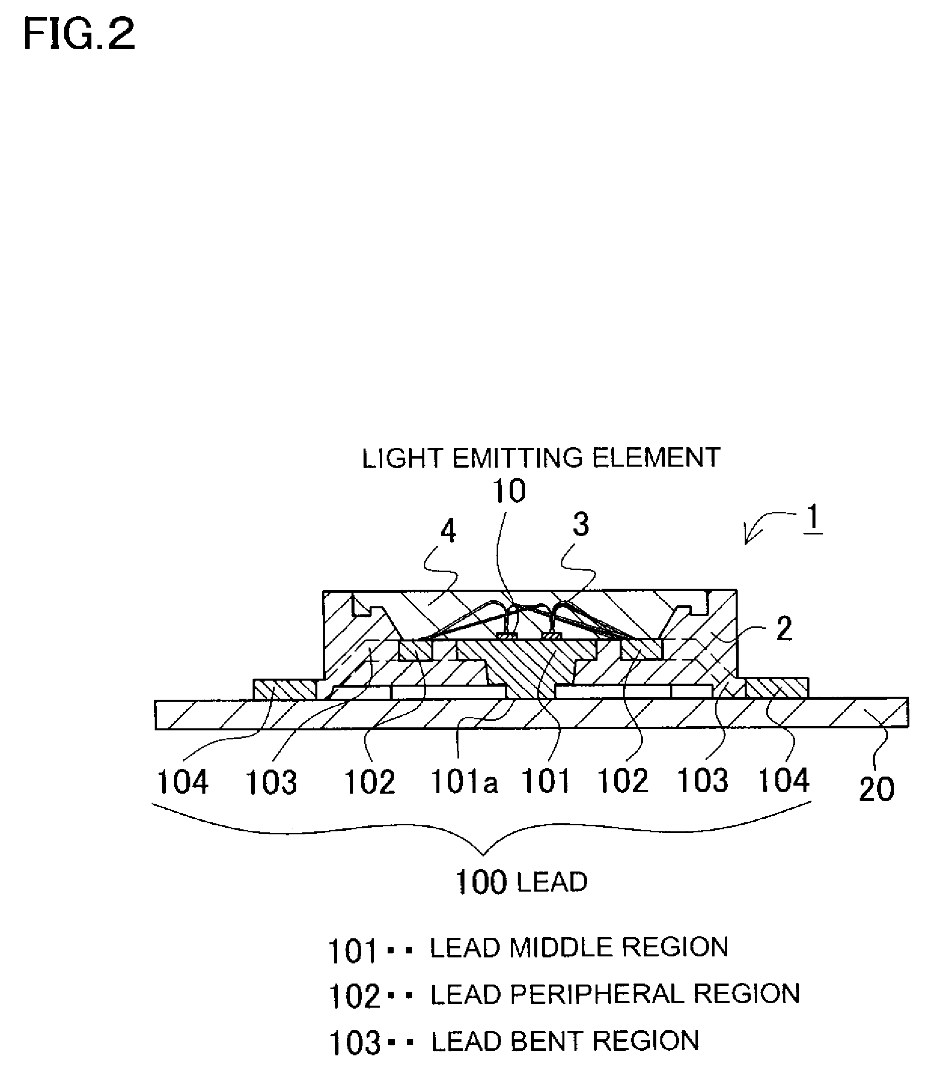
[0049]FIG. 1 is a perspective view showing a semiconductor light emitting device 1 according to a first embodiment. FIG. 2 is a cross-sectional view of the semiconductor light emitting device 1 of FIG. 1 taken along the line II-II′. The semiconductor light emitting device 1 according to the first embodiment is now schematically described with reference to FIGS. 1 and 2. The semiconductor light emitting device 1 is provided with a package 2 that is mounted on lead arrangement 100. The package 2 has space that is formed in a substantially recessed shape and opens upward. In addition, a plurality of light emitting elements 10 are mounted on an exposed part of the lead arrangement 100 inside the space of the package 2. That is, the package 2 serves as a frame body that surrounds the light emitting elements 10. Additionally, a protection element 5 such as Zener diode 5 is also mounted inside the opening space of the package 2. The protection element 5 provides electrical conduction when ...

second embodiment

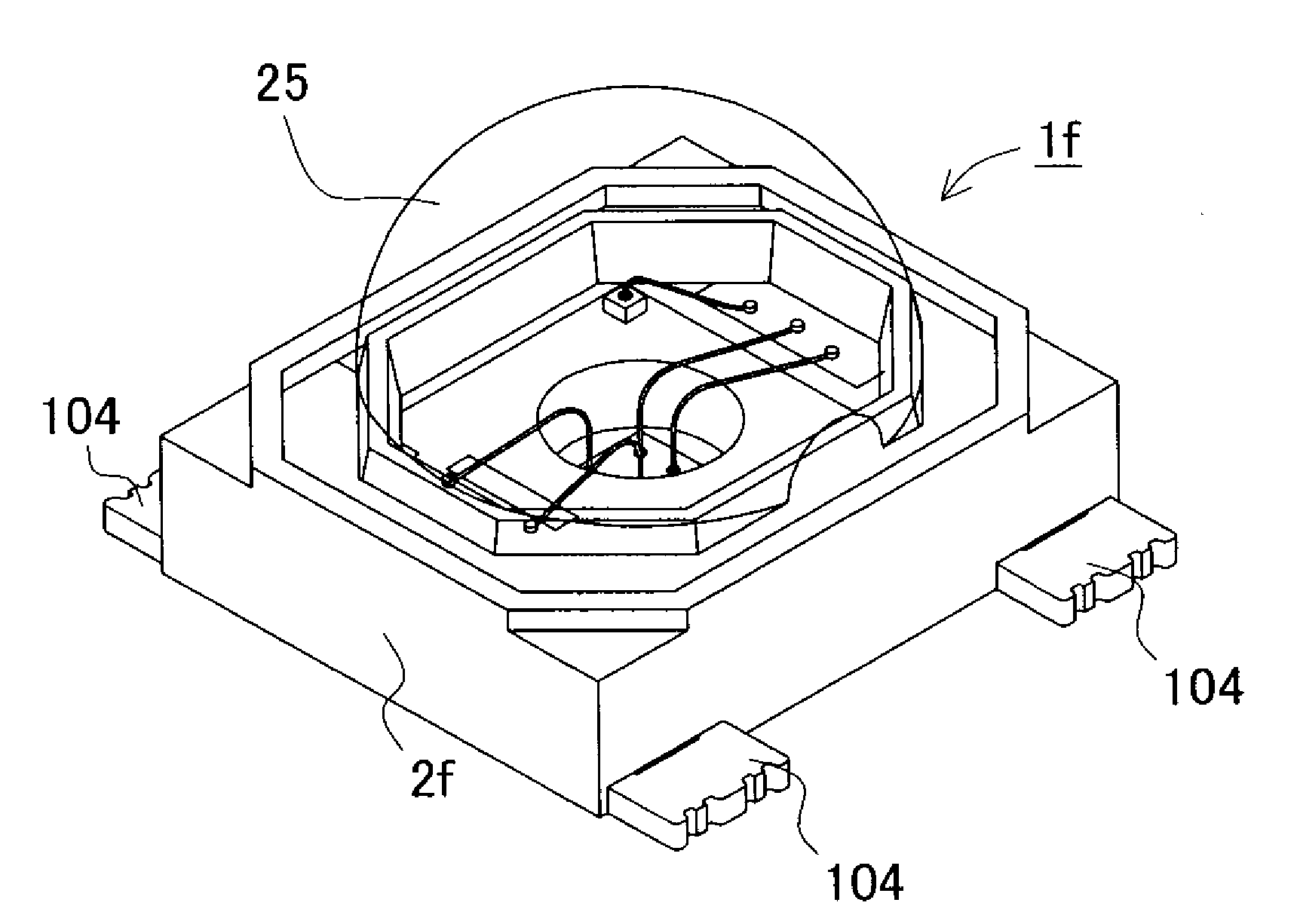
[0114]FIG. 12 shows a lens-attached semiconductor light emitting device 1b. FIG. 12(a) is a perspective view showing the lens-attached semiconductor light emitting device 1b as viewed from the top side. FIG. 12(b) is a perspective view showing the lens-attached semiconductor light emitting device 1b as viewed from the bottom side. The lens-attached semiconductor light emitting device 1b is similar to the semiconductor light emitting device 1 or 1a according to the first embodiment except that a dome-shaped lens 22 is additionally attached on the light emission surface side. The dome-shaped lens has a dome shape such as hemisphere. The members same as the semiconductor light emitting device 1 or 1a according to the first embodiment can be used except for this lens.

[0115]As shown in FIG. 12(a), the dome-shaped lens 22 according to this second embodiment is attached so as to cover the light emission surface, i.e., an upper middle part of the semiconductor light emitting device 1 in FIG...

third embodiment

[0117]FIG. 13 shows another lens-attached semiconductor light emitting device 1c. FIG. 13(a) is a perspective view showing the lens-attached semiconductor light emitting device 1c as viewed from the top side. FIG. 13(b) is a perspective view showing the lens-attached semiconductor light emitting device 1c as viewed from the bottom side. The semiconductor light emitting device 1c is similar to the semiconductor light emitting device 1 or 1a according to the first embodiment except that a Fresnel lens 24 is additionally attached on the light emission surface side. The Fresnel lens has concentrically narrow circular stepped lens setbacks that are divided from a convex surface of planoconvex lens, and has a small thickness but provides a thicker convex lens function. The members same as the semiconductor light emitting device 1 or 1a according to the first embodiment can be used except for this lens.

[0118]Similarly to the second embodiment, the Fresnel lens 24 includes projections at fo...


PUM


Abstract

Both ends of the lead arrangement project outward from side surfaces of a package to form outer lead regions. Each of the outer lead regions includes a pair of outer lead projections and lead terminal smaller projections that are located between the outer lead projections. The outer lead projections and lead terminal smaller projections project outward. Adjustment is made to the projection amount of end surfaces of the lead smaller projections lying in a plane perpendicular to a longitudinal direction of the lead arrangement, whereby the end surfaces projecting less than end surfaces of the outer lead projections. Thus, cut surfaces of lead connection portions with edged corners are not exposed. This arrangement prevents that the cut surfaces damage other devices.

Description

BACKGROUND OF THE INVENTION[0001]1. Field of the Invention[0002]The present invention relates to a semiconductor light emitting device, and a method for producing it.[0003]2. Description of the Related Art[0004]FIG. 17 is a perspective view showing one production process of a conventional LED light emitting device 200. FIG. 18 is a cross-sectional view showing the LED light emitting device 200. The LED light emitting device 200 includes a package 206 and a lead 205, as shown in FIG. 8. The package 206 includes space that opens upward and has a substantially inverted truncated cone shape. The lead 205 is made of a conductive material and is fixedly attached to the package 206. The lead 205 includes a lead middle portion 205b that is located in a substantially middle part of the light emitting device, and a lead terminal portion 205a that projects outward of the package 206. When the lead 205 and the package 206 are fixedly attached, the lead middle portion 205b that is a part of the ...

Claims


Application Information

Patent Timeline
Patent Type & Authority Applications(United States)
IPC IPC(8): H01L33/00H01L33/32H01L33/56H01L33/58H01L33/62
CPCH01L24/45H01L25/0753H01L2924/12041H01L2224/49113H01L24/97H01L2924/01028H01L2924/01013H01L2224/48465H01L2924/01322H01L2924/19041H01L2924/01079H01L2924/01078H01L2924/01064H01L33/486H01L33/62H01L2224/45144H01L2224/48091H01L2224/48247H01L2224/48257H01L2924/01004H01L2924/01014H01L2924/0102H01L2924/01046H01L2924/0105H01L2924/01057H01L2924/01058H01L2924/00014H01L2924/00H01L2924/351H01L2924/15787H01L2924/12035H01L2924/12036H01L2924/12043H01L2924/181
Inventor BANDO, YOSHITAKA
Owner NICHIA CORP
Why Eureka
Try Eureka