Optical transmitter

a technology of optical transmitter and optical level, applied in the field of optical transmitter, can solve the problems of delay shift in optical level cannot be compensated, signal deterioration, signal deterioration, etc., and achieve the effect of stably sending high-quality optical signals

Inactive Publication Date: 2007-11-15
FUJITSU LTD
View PDF7 Cites 38 Cited by
  • Summary
  • Abstract
  • Description
  • Claims
  • Application Information

AI Technical Summary

Benefits of technology

[0040]In the optical transmitter of the above described configuration, a part of the optical signal having been subjected to multivalued phase modulation and pulsing in the first and the second optical modulators is branched by the output monitor section, the power of the low frequency component including the DC component in the electrical spectrum acquired by photoelectrically converting the branched beams is measured, and the relative phase of respective drive signals applied to the first and the second optical modulators is then feed-back controlled by the controller

Problems solved by technology

In such a modulation format using the plurality of optical modulators, there is a problem in that a change in the optical signal delay generated between the plurality of optical modulators may cause signal deterioration.
However, the above conventional technique is a method for directly monitoring drive signals applied to a plurality of modulators to detect a relative phase relation (delay difference), and performing feed-back control based on the detection result, and has a problem in that a delay shift in the optical level cannot be compensated, though a delay shift in the electrical level can be compensated.
Therefore, if a delay shift of the PMF occurs due to a temperature change as shown in FIG. 18, the delay shift due to the temperature change becomes a value which cannot be ignored, as compared with the tolerance, thereby causing signal deterioration.
Moreover, not only the temperature variant delay amount in the PMF for connecting the plurality of optical modulators, but also a temperature variant delay amount in an electronic circuit or an electric signal transmis

Method used


Image

  • Optical transmitter
  • Optical transmitter
  • Optical transmitter

Examples


first embodiment

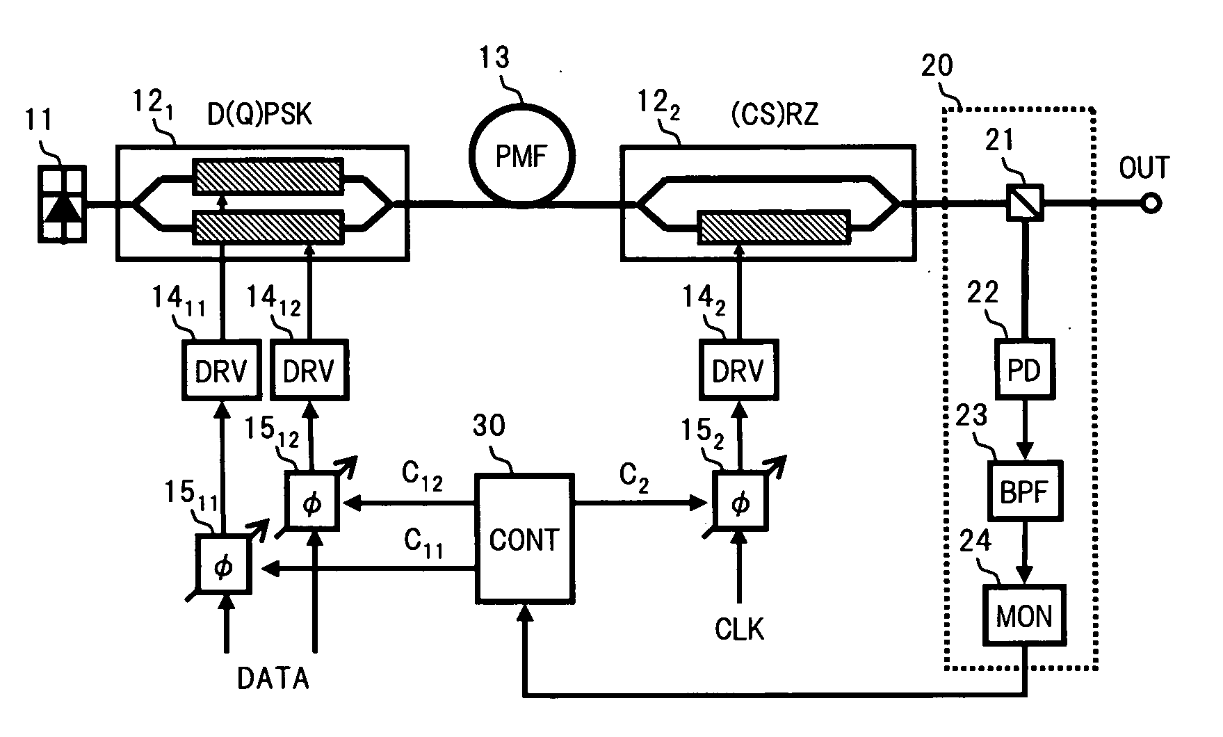
[0063]FIG. 1 is a block diagram showing an optical transmitter according to the present invention.

[0064]In FIG. 1, in the optical transmitter of the first embodiment, for example, a multivalued optical phase modulator 121 serving as a first optical modulator driven according to a data signal DATA, and a (CS)RZ pulsing intensity modulator 122 serving as a second optical modulator driven according to a clock signal CLK, are serially connected via a polarization maintaining optical fiber (PMF) 13 between a CW light source 11 and an output port OUT. Moreover, the optical transmitter includes an output monitor section 20 which acquires an electrical spectrum by branching a part of a (CS)RZ-D(Q)PSK-modulated optical signal output from the post-stage intensity modulator 122 to the output port OUT as a monitor light, and then photoelectrically converting the monitor light, and measures a power change of a pre-set frequency component, excluding a frequency component corresponding to a baud r...

second embodiment

[0075]Next is a description of the present invention.

[0076]FIG. 8 is a block diagram showing the second embodiment of the optical transmitter according to the present invention.

[0077]In FIG. 8, the point where the configuration of the optical transmitter in the second embodiment is different from the case of the first embodiment shown in FIG. 1 is that a low-pass filter (LPF) 25 and a capacitor 26 are provided between the photodetector 22 and the power monitor 24, instead of the band-pass filter 23 in the output monitor section 20. The low-pass filter 25 is an electric filter in which a cutoff frequency is set on the lower frequency side than the vicinity of 22 GHz, for example, relative to the 44 GHz (CS)RZ-D(Q)PSK signal light. Here 10 MHz is assumed as a preferable setting example of the cutoff frequency. However, the cutoff frequency of the low-pass filter 25 in the present invention is not limited to the above specific example. The capacitor 26 intercepts the DC component of th...

third embodiment

[0083]Next is a description of the present invention.

[0084]In FIG. 10, the point where the configuration of the optical transmitter in the third embodiment is different from the case of the first embodiment shown in FIG. 1 is that the low-pass filter (LPF) 25 is provided between the photodetector 22 and the power monitor 24, instead of the band-pass filter 23 in the output monitor section 20. The low-pass filter 25 is an electric filter in which a cutoff frequency is set on the lower frequency side than the vicinity of 22 GHz, for example, relative to the 44 GHz (CS)RZ-D(Q)PSK signal light. Here 10 MHz is assumed as a preferable setting example of the cutoff frequency. However, the cutoff frequency of the low-pass filter 25 in the present invention is not limited to the specific example. The power monitor 24 used here measures the power including both the DC component and the AC component of the input electric signal.

[0085]FIG. 11 is a diagram showing an example in which a relation ...


PUM


Abstract

In an optical transmitter of the invention, continuous light from a light source is a (CS)RZ-D(Q)PSK modulated by two optical modulators connected in series, and a part of the optical signal output from a post-stage optical modulator is branched by an output monitor section, and the power of a preset frequency component, excluding a frequency component corresponding to a baud rate, included in an electrical spectrum acquired by photoelectrically converting the branched beams is measured. The relative phase of drive signals applied to the optical modulators is then feed-back controlled so that the power becomes a minimum. As a result, a delay shift due to a temperature change or the like between drive signals applied to respective optical modulators, can be reliably compensated.

Description

BACKGROUND OF THE INVENTION[0001]1. Field of the Invention[0002]The present invention relates to an optical transmitter that transmits pulsed multivalue phase-modulated light, and more specifically, relates to an optical transmitter capable of compensating a phase shift due to a temperature change or the like between drive signals, respectively applied to a plurality of serially connected light modulation sections.[0003]2. Related Art[0004]Recently, demand for the introduction of a next generation 40 Gbit / s optical transmission system has increased, and transmission distance and frequency efficiency equivalent to those of a 10 Gbit / s system are also required. As a means for realizing this, research and development of Return to Zero-Differential Phase Shift Keying (RZ-DPSK) modulation or Carrier Suppressed Return to Zero-Differential Phase Shift Keying (CSRZ-DPSK) modulation, which are excellent in optical signal-to-noise ratio (OSNR) resistance and nonlinearity resistance as compare...

Claims


Application Information

Patent Timeline
IPC IPC(8): H04B10/04H04B10/516H04B10/07H04B10/556H04B10/58H04B10/61H04L27/20
CPCH04B10/5051H04B10/58H04B10/50577H04B10/5057
Inventor YUKI, MASAHIRONAKAMURA, KENTAROOOI, HIROKINISHIHARA, MASATO
Owner FUJITSU LTD
Why Eureka
Try Eureka