Method and apparatus for pattern inspection

a pattern inspection and pattern technology, applied in the direction of instruments, image enhancement, therapy, etc., can solve the problems of long scanning time, difficult to obtain the required defect detection sensitivity, disadvantages that will become substantial obstacles to reducing inspection time, etc., to prevent the delay of a semiconductor device manufacturing line, inspection speed, and inspection of defects

Inactive Publication Date: 2007-11-29
HITACHI HIGH-TECH CORP
View PDF7 Cites 31 Cited by
  • Summary
  • Abstract
  • Description
  • Claims
  • Application Information

AI Technical Summary

Benefits of technology

[0014] According to the present invention, therefore, it is possible to set such conditions as optimized pixel size, illuminating area size, etc. to easily realize an inspection speed capable of preventing an semiconductor device manufacturing line from delay so that the user can inspect defects of each semiconductor pattern efficiently under optimized conditions. Because such inspection conditions can be set easily such way, the total inspection time from condition setting to end of inspection can be reduced. And because the apparatus can be operated easily, the apparatus will also have advantages in sales policy.

Problems solved by technology

However, because the SEM type inspection apparatus scans an electron beam on a specimen surface two-dimensionally to obtain an image, the scanning time is long.
This disadvantage will become a substantial obstacle for reducing the inspection time.
On the other hand, a secondary electron mapping type inspection apparatus cannot obtain a sufficient resolution due to the aberration of the objective lens, thereby it is difficult to obtain a required defect detection sensitivity.

Method used


Image

  • Method and apparatus for pattern inspection
  • Method and apparatus for pattern inspection
  • Method and apparatus for pattern inspection

Examples


first embodiment

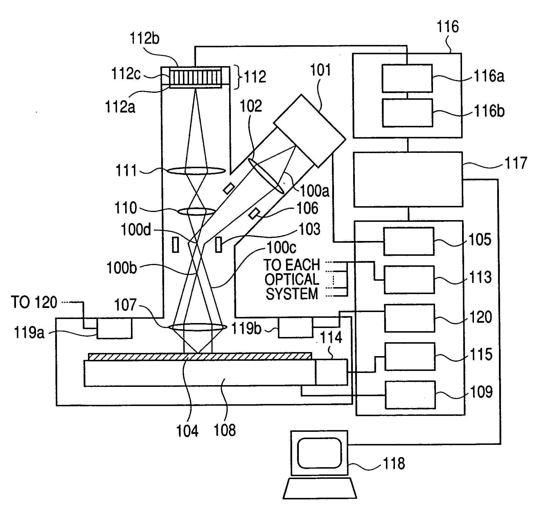
[0026]FIG. 1 shows an example of a hardware configuration of the mirror electron imaging type wafer inspection apparatus in the preferred embodiment of the present invention. In FIG. 1, vacuum pumps, their controller, pipes for evacuating systems, etc. are omitted.

[0027] At first, main elements of the electron optical system of the apparatus will be described. An illuminating electron beam 100a emitted from an electron gun 101 is focused by a condenser lens 102 and deflected by an ExB deflector 103 to form a cross-over 100b, then illuminated onto a specimen wafer 104 as an approximate parallel flux. In FIG. 1, although only one condenser lens 102 is used, a plurality of lenses may be combined into a lens system to optimize the optical conditions. The electron gun 101 is usually a Zr / 0 / W type Schottky electron source. Such voltages and currents as an extracting voltage applied to the electron gun 101, an accelerating voltage to extracted electrons, a heating current of an electron s...

second embodiment

[0042] In the first embodiment, the user determines conditions for operating the inspection apparatus with reference to mainly the values of inspection speed and pixel size and the relationship between the defect detection sensitivity and the pixel size is not clear. In this second embodiment, therefore, the horizontal axis of the graph displayed on the inspection speed S setting screen is used for defect detection sensitivity, thereby the user comes to know the relationship between the defect detection sensitivity and the pixel size intuitively. Instead of the horizontal axis, the vertical axis may also be used for the defect detection sensitivity.

[0043]FIG. 5 shows a schematic diagram of the inspection speed S setting screen displayed on the user interface device with a monitor 118 of the mirror electron imaging type wafer inspection apparatus. The user operation screen shown in FIG. 5 is displayed on the monitor of the mirror electron imaging type wafer inspection apparatus or m...

third embodiment

[0052] In the second embodiment, a description is made for a user operation screen on which the defect magnification is set as 3 times. This third embodiment enables the user to change the defect magnification.

[0053]FIG. 9 shows a user operation screen in this third embodiment. The user operation screen shown in FIG. 9 is displayed on the monitor of the mirror electron imaging type wafer inspection apparatus or mirror electron imaging type specimen inspection apparatus. In this third embodiment, the description for the same components as those shown in FIG. 5 will be omitted. In FIG. 9, there is only a difference from that shown in FIG. 5; a defect magnification selection field 901 is provided. The user can select a magnification from a plurality of defect magnification values by clicking the arrow in the defect magnification selection field 901. The value of the horizontal axis of the graph 902 is corrected by the selected defect magnification, thereby the displayed characteristic...


PUM

PropertyMeasurementUnit
areaaaaaaaaaaa
areaaaaaaaaaaa
voltageaaaaaaaaaa

Abstract

Because a mirror electron imaging type inspection apparatus for obtaining an inspection object image with mirror electrons has been difficult to optimize inspection conditions, since the image forming principles of the apparatus are different from those of conventional SEM type inspection apparatuses. In order to solve the above conventional problem, the present invention has made it possible for the user to examine such conditions as inspection speed, inspection sensitivity, etc. intuitively by displaying the relationship among the values of inspection speed S, inspection object digital signal image pixel size D, inspection object image size L, and image signal acquisition cycle P with use of a time delay integration method as a graph on an operation screen. The user can thus determine a set of values of a pixel size, an inspection image width, and a TDI sensor operation cycle easily with reference to the displayed graph.

Description

CLAIM OF PRIORITY [0001] The present application claims priority from Japanese application JP 2006-027861 filed on Feb. 6, 2006, the content of which is hereby incorporated by reference into this application. FIELD OF THE INVENTION [0002] The present invention relates to a method and an apparatus for inspecting an electrical defect of a microstructure circuit formed on a semiconductor wafer. BACKGROUND OF THE INVENTION [0003] As a method for detecting a defect of a circuit pattern formed on a wafer by comparing images in a manufacturing process of a semiconductor device, for example, a pattern comparing inspection method is disclosed in JP-A No. 258703 / 1993. The method uses an SEM in which, a point focused electron beam is scanned. The SEM type inspection apparatus is higher in resolution than optical inspection systems and it has a feature for enabling such an electrical defect as a connecting failure to be detected. However, because the SEM type inspection apparatus scans an elect...

Claims


Application Information

Patent Timeline
Patent Type & Authority Applications(United States)
IPC IPC(8): G01N23/00
CPCH01J37/29H01J2237/22H01J2237/24592H01J37/265G06T2207/10056G06T2207/30148G06T7/0004
Inventor HASEGAWA, MASAKIMURAKOSHI, HISAYAMAKINO, HIROSHI
Owner HITACHI HIGH-TECH CORP
Why Eureka
Try Eureka