
Conductive paste and method of manufacturing electronic component using the same

a technology of electronic components and conductive paste, which is applied in the direction of non-conductive materials with dispersed conductive materials, semiconductor devices, and non-conductive materials, etc., can solve the problems of weak bonding force at the interface between the electrode and the piezoelectric member, the ion migration is suppressed to some degree but not practicable, and the electrode formed of metals such as gold or platinum showed a poor adhesion property between the electrode and the piezoelectric member, the electric resistance of the electrode resistance resistan

Inactive Publication Date: 2007-11-29
ALPS ALPINE CO LTD
View PDF6 Cites 2 Cited by
  • Summary
  • Abstract
  • Description
  • Claims
  • Application Information

AI Technical Summary

Benefits of technology

[0012] The embodiments described herein solve the problems in the above-mentioned related art. Particularly, an object of the invention is to provide a conductive paste capable of realizing both excellent adhesion property and low electric resistance between the electrode and a substrate (a piezoelectric member) and preventing generation of cracks in the substrate and a method of manufacturing an electronic component using the conductive paste.

Problems solved by technology

In the case of the conductive film containing palladium in addition to the silver, the ion migration is suppressed to some degree but not practically usable.
However, the electrode formed of metals such as gold or platinum showed very poor adhesion property between the electrode and a piezoelectric member.
However, since the gold or platinum is a metal that is hardly oxidized, that is, hardly combines with oxygen, the bonding force at an interface between the electrode and the piezoelectric member becomes weak even when the electrode of gold is formed on the piezoelectric member.
However, even in the case of the electrode formed of the metal resinate, the adhesion property between the electrode and the piezoelectric member was not improved appropriately.

Method used


Image

  • Conductive paste and method of manufacturing electronic component using the same
  • Conductive paste and method of manufacturing electronic component using the same
  • Conductive paste and method of manufacturing electronic component using the same

Examples


examples

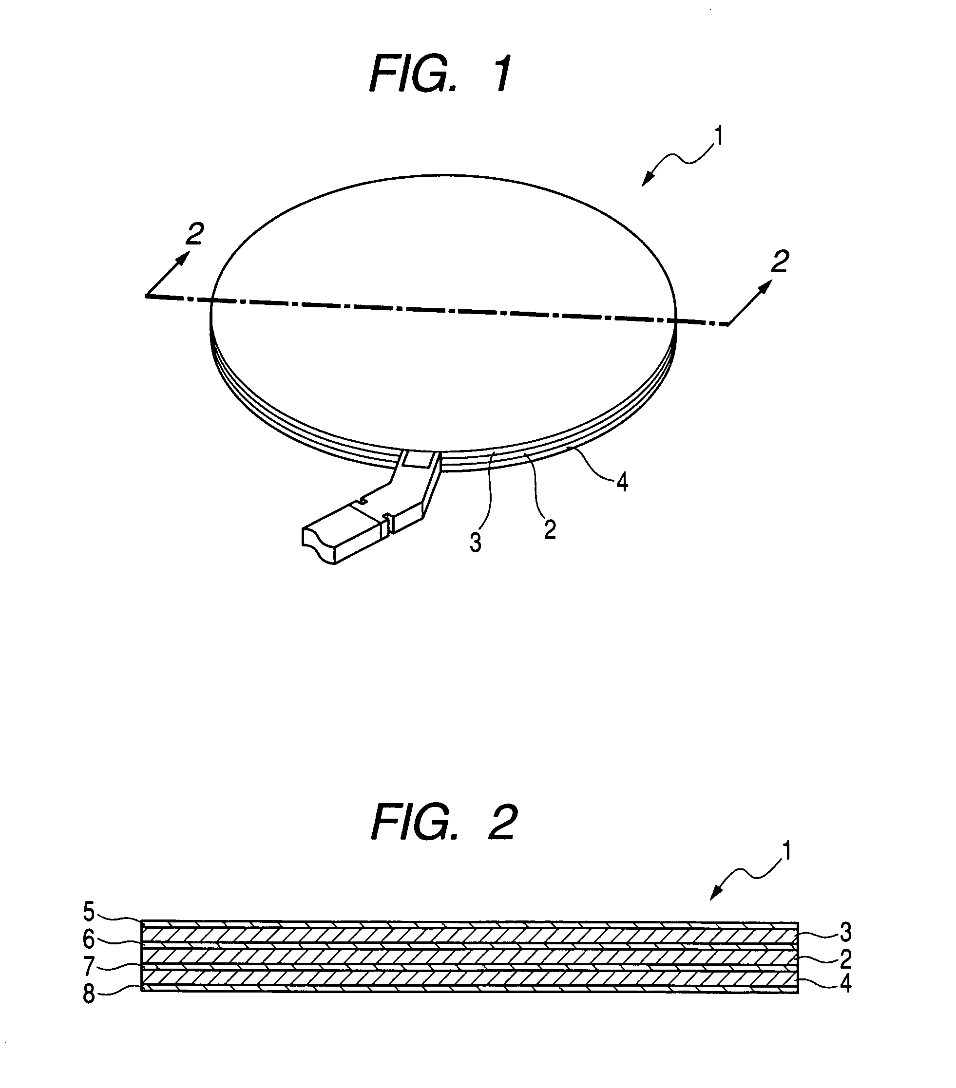
[0058] Conductive pastes of the composition shown in the following Table 1 were applied to an entire surface of a circular substrate expressed by [Pb(Zr1 / 2Ti1 / 2)O3]0.6+[Pb(Zn1 / 3Nb2 / 3)O3]0.16+[Pb(Ni1 / 3Nb2 / 3)O3]0.24 (about 28 mm in diameter) (a piezoelectric member) by screen-printing and then baked at 650° C. for 30 minutes so as to form electrodes. A centerline average roughness Ra of the surface of the substrate was in the range of 0.1 to 0.2 μm in all samples.

[0059] A tape having a predetermined adhesion property was attached to the electrode, and a peel test was carried out for measuring whether the electrode was peeled away from the substrate at the time of removing the tape.

TABLE 1Tape adhesion propertyConductive157 gf / cm288 gf / cm438 gf / cmSamplepasteInitialInitialInitialAfterNo.compositionstageAfter teststageAfter teststagetestExample 1Gold resinate0 / 100 / 10—6 / 10—0 / 10Example 2Gold resinate0 / 100 / 10—4 / 10—0 / 10and 4% of fineglass powderExample 3Gold resinate0 / 100 / 10—2 / 10—0 / 10and ...


PUM


Abstract

Exemplary embodiments provided a conductive paste including an organic gold compound and a glass component in a solvent. When electrodes are formed on both surfaces of piezoelectric members using the conductive paste according to the invention, it is possible to improve the close adhesion property between the electrodes and the piezoelectric members eliminate ion migration, and lower electric resistances of the electrodes.

Description

[0001] This application claims the benefit of Japanese Patent Application No. 2006-135325, filed on May 15, 2006, the content of which is incorporated herein by reference. BACKGROUND OF THE INVENTION [0002] 1. Field of the Invention [0003] The present invention relates to a conductive paste used in, for example, an electrode of a bimorph-typeora unimorph piezoelectric element, and more particularly, to a conductive paste capable of realizing both excellent adhesion property and low electric resistance between the electrode and a substrate (a piezoelectric member) and preventing generation of cracks in the substrate and a method of manufacturing an electronic component using the conductive paste. [0004] 2. Description of the Related Art [0005] A conductive film containing silver is used as an electrode material of a piezoelectric element. The piezoelectric element may be used as a diaphragm of a coolant circulation pump. [0006] However, ion migration of the silver is caused in the el...

Claims


Application Information

Patent Timeline
IPC IPC(8): H01L47/00H01L39/22H01B1/20H01L41/09H01L41/187H01L41/22H01L41/29
CPCH01B1/16H01L41/0973H01L41/047H10N30/878H10N30/2047
Inventor ONISHI, HITOSHIYAMADA, SATOSHISEKIGUCHI, AKIRA
Owner ALPS ALPINE CO LTD
Learn More