Organic light emitting device and organic electronic device

Inactive Publication Date: 2007-11-29
SAMSUNG SDI CO LTD
View PDF0 Cites 57 Cited by
  • Summary
  • Abstract
  • Description
  • Claims
  • Application Information

AI Technical Summary

Benefits of technology

[0010]The present invention provides an organic light emitting device having a structure in which the penetration of harmful elements into an inner functional layer i

Problems solved by technology

The second electrode layer 25 readily corrodes or oxidizes by reacting with external oxygen due to its characteristics of high activity and chemical instability.
However, the sealing can 30 increases the weight and volume of a display device, and is a limiting factor for making a light-weight, thin, small display device.
Therefore, there is a structural limitation in using the can type sealing method on large scale display devices that are 2 inches or more in size.
Thus, external harmful materials penetrate the inner side

Method used


Image

  • Organic light emitting device and organic electronic device
  • Organic light emitting device and organic electronic device
  • Organic light emitting device and organic electronic device

Examples


Example

[0038]The present invention is described more fully below with reference to the accompanying drawings in which exemplary embodiments of the present invention are shown.

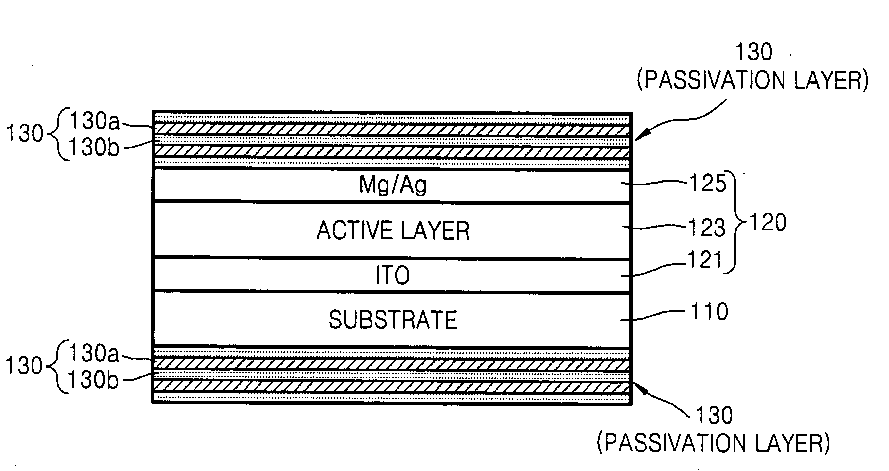
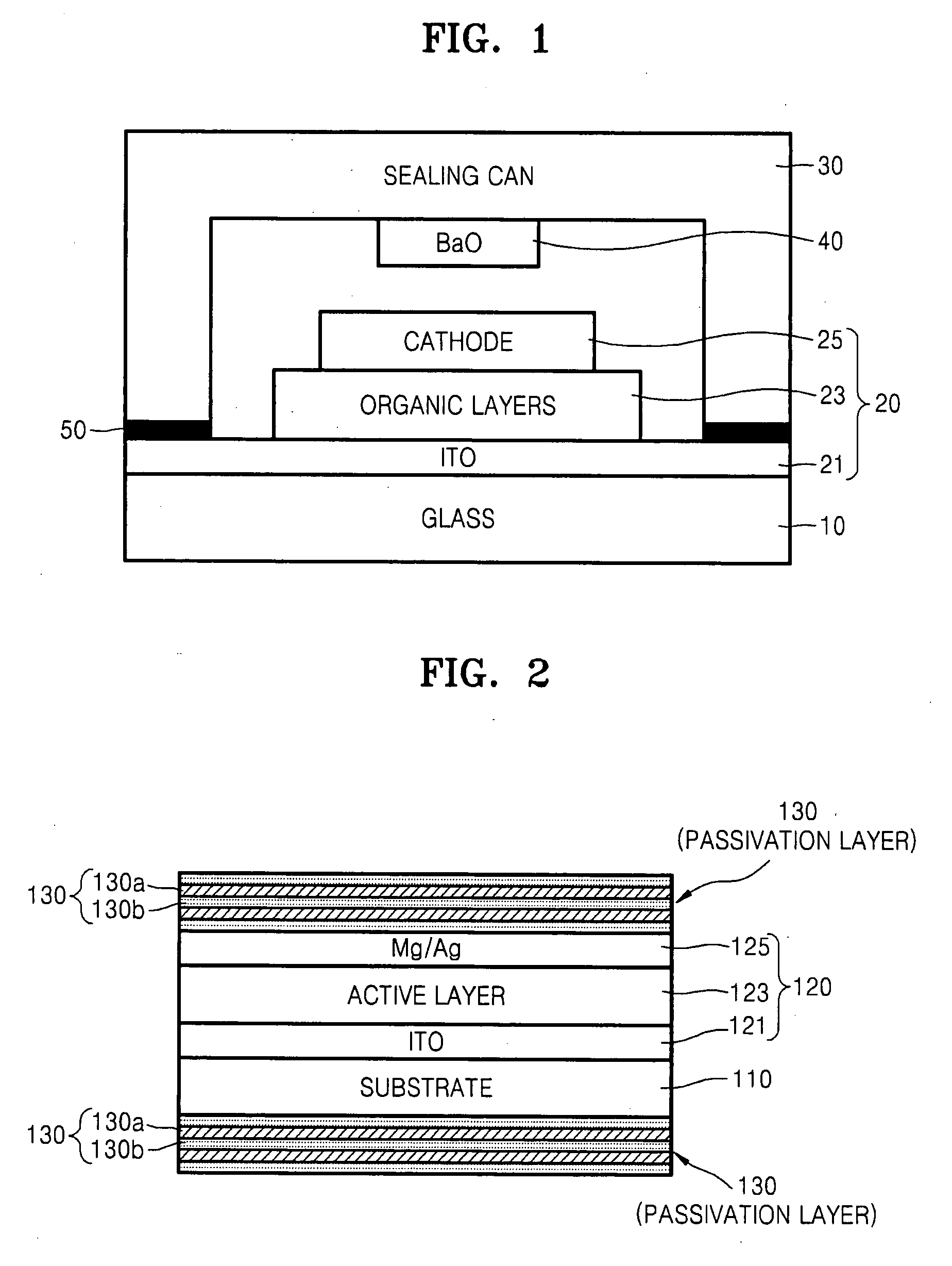
[0039]FIG. 2 is a vertical cross-sectional view of an organic light emitting device according to an embodiment of the present invention.

[0040]Referring to FIG. 2 and FIG. 4, the organic light emitting device includes an insulating substrate 110, a light emitting unit 120 formed on the insulating substrate 110, and a passivation layer 130 that seals the light emitting unit 120 to protect the light emitting unit 120 from harmful materials. The insulating substrate 110 can be formed of a hard material, such as glass, stainless steel, or aluminum, or alternatively, can be formed of a soft material, such as Polyethylene Terephthalate (PET), Polyethylene Naphthalate (PEN), Polyether Sulfone (PES), Polyimide, Polypropylene, cellophane, PVC, etc. in order to have flexibility.

[0041]The light emitting unit 120 displays a predet...


PUM


Abstract

An organic light emitting device has a structure in which the penetration of harmful materials into an inner functional layer is blocked to prevent the degradation of the performance of the organic light emitting device and an organic electronic device includes such an organic light emitting device. The organic light emitting device includes an insulating substrate; a light emitting unit arranged on the insulating substrate and including a first electrode layer to inject holes, a second electrode layer to inject electrons, and an active layer interposed between the first and second electrode layers to emit light by recombining the holes and electrons; and a passivation layer including alternately arranged barrier layers and buffer layers to seal the light emitting unit from an external atmosphere, each barrier layer including at least one material selected from a group consisting of an activated metal oxide, an activated metal nitride, or an activated metal oxynitride, and each buffer layer being of a polymer organic material.

Description

CLAIM OF PRIORITY[0001]This application makes reference to, incorporates the same herein, and claims all benefits accruing under 35 U.S.C. § 119 from an application for ORGANIC LIGHT EMITTING DEVICE AND ORGANIC ELECTRONIC DEVICE earlier filed in the Korean Intellectual Property Office on 25 May 2006 and there duly assigned Serial No. 10-2006-0047221.BACKGROUND OF THE INVENTION[0002]1. Field of the Invention[0003]The present invention relates to an organic light emitting device and an organic electronic device, and more particularly, the present invention relates to an organic light emitting device having a structure in which the penetration of a harmful element into an inner functional layer is shielded in order to prevent the degradation of the performance of the organic light emitting device and an organic electronic device.[0004]2. Description of the Related Art[0005]FIG. 1 is a vertical cross-sectional view of an organic light emitting device. Referring to FIG. 1, a first electr...

Claims


Application Information

Patent Timeline
IPC IPC(8): H05B33/22H01L51/50
CPCH01L51/5237H10K50/84H10K50/8445H05B33/04
Inventor KIM, SANG-YEOLPARK, JONG-JINPU, LYONG-SUNPARK, JOON-YONGSON, YOUNG-MOKLEE, SUNG-HUNKIM, MU-GYEOMLEE, TAE-WOO
Owner SAMSUNG SDI CO LTD
Why Eureka
Try Eureka