Method of manufacturing semiconductor device

a manufacturing method and semiconductor technology, applied in semiconductor devices, photomechanical treatment, instruments, etc., can solve problems such as misalignment of pattern, difficulty in detection of alignment marks placed under bit line layers, and circuits not being fabricated as designed

Inactive Publication Date: 2007-11-29
LONGITUDE SEMICON S A R L
View PDF4 Cites 214 Cited by
  • Summary
  • Abstract
  • Description
  • Claims
  • Application Information

AI Technical Summary

Benefits of technology

[0036]As set forth above, in the method of manufacturing the semiconductor device according to the present invention, after the alignment mark layer made of the conductive substance is covered with the interlayer insulating film, the mark hole is formed in the interlayer insulating film laid in the alignment mark section, so as to expose the alignment mark layer. Further, in forming the mark hole, the insulating film laid under the alignment mark layer is together worked upon in the manner of self-alignment, providing, beforehand, a difference in level for the alignment mark, which is to be formed consisting of a multi-layered film comprising the insulating film and the conductive substance layer. Subsequently, the bit line layer is formed of metal or the like. The metal is reflected in the difference in level, which is to be formed consisting of a multi-layered film comprising the insulating film and the conductive substance layer so that the resulting structure becomes equivalent to the one that the metal itself has the difference in level. Therefore, the difference in level made of metal appears on the surface and the mark detection light has the contrast induced by the difference in level made of metal. To be short, the present invention has the effect that the alignment of the upper layer pattern with the lower layer pattern becomes possible, regardless of the presence of metal, which is opaque to the visible light, between the lower layer alignment mark and the upper layer photoresist.

Problems solved by technology

However, once a bit line layer made of a metal film such as a tungsten film is formed on the planarized surface of the interlayer insulating film 14, the detection of the alignment mark which is placed under the bit line layer becomes difficult, since the metal constituting the bit line layer is opaque to the visible light used for the alignment mark detection.
Therefore, the bit line 17 can not be aligned with the contact plug 13 during the formation, causing a misalignment of the pattern and giving rise to a problem that circuits may not be fabricated as designed.
As described above, when the alignment mark is made with the contact plug layer which is formed at a higher level than the word line, and a pattern is formed at an even higher level using this alignment mark, the presence of a film of metal or the like, which is opaque to the visible light, between the alignment mark and the upper layer photoresist makes the alignment mark detection difficult, and brings about serious problems in alignment between the upper layer and the lower layer and consequently in circuit construction.

Method used


Image

  • Method of manufacturing semiconductor device
  • Method of manufacturing semiconductor device
  • Method of manufacturing semiconductor device

Examples


example

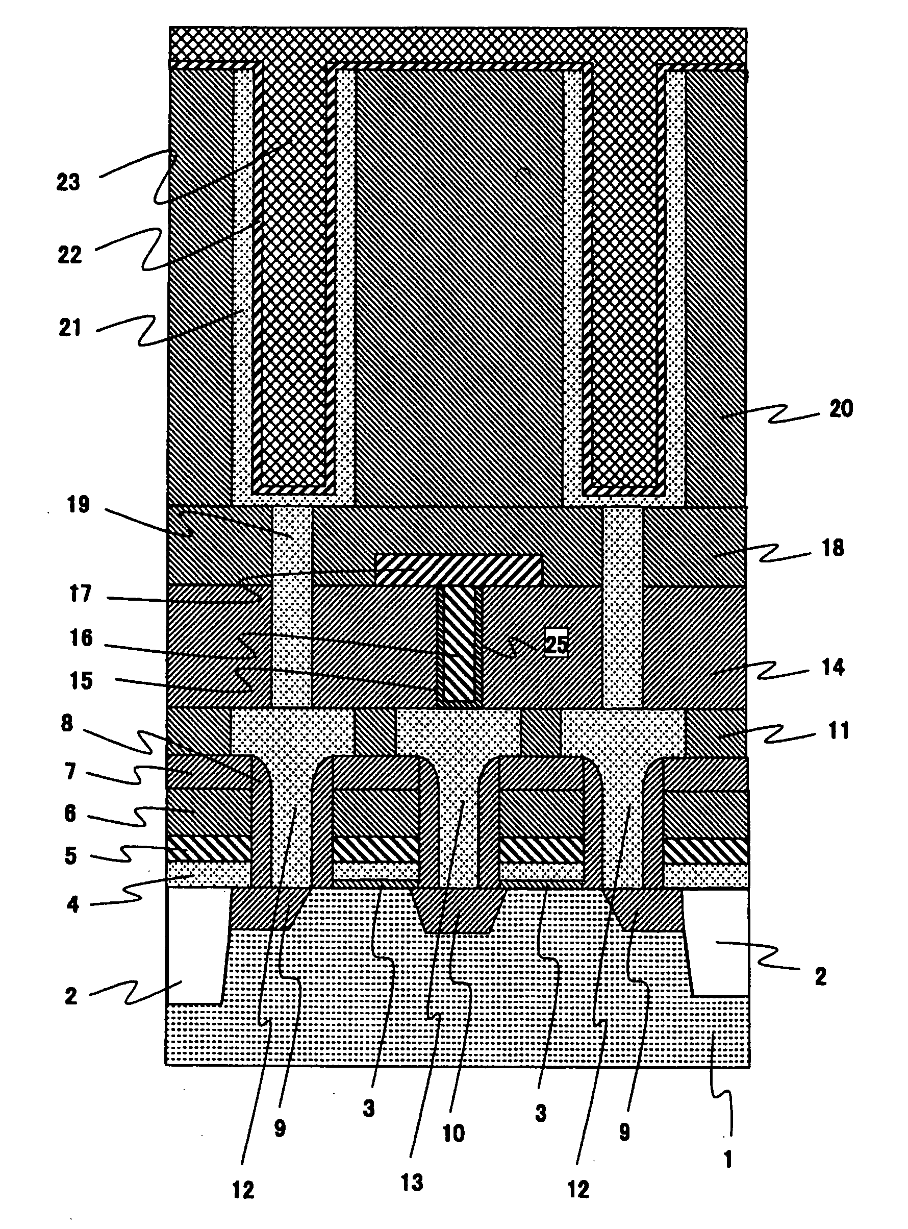
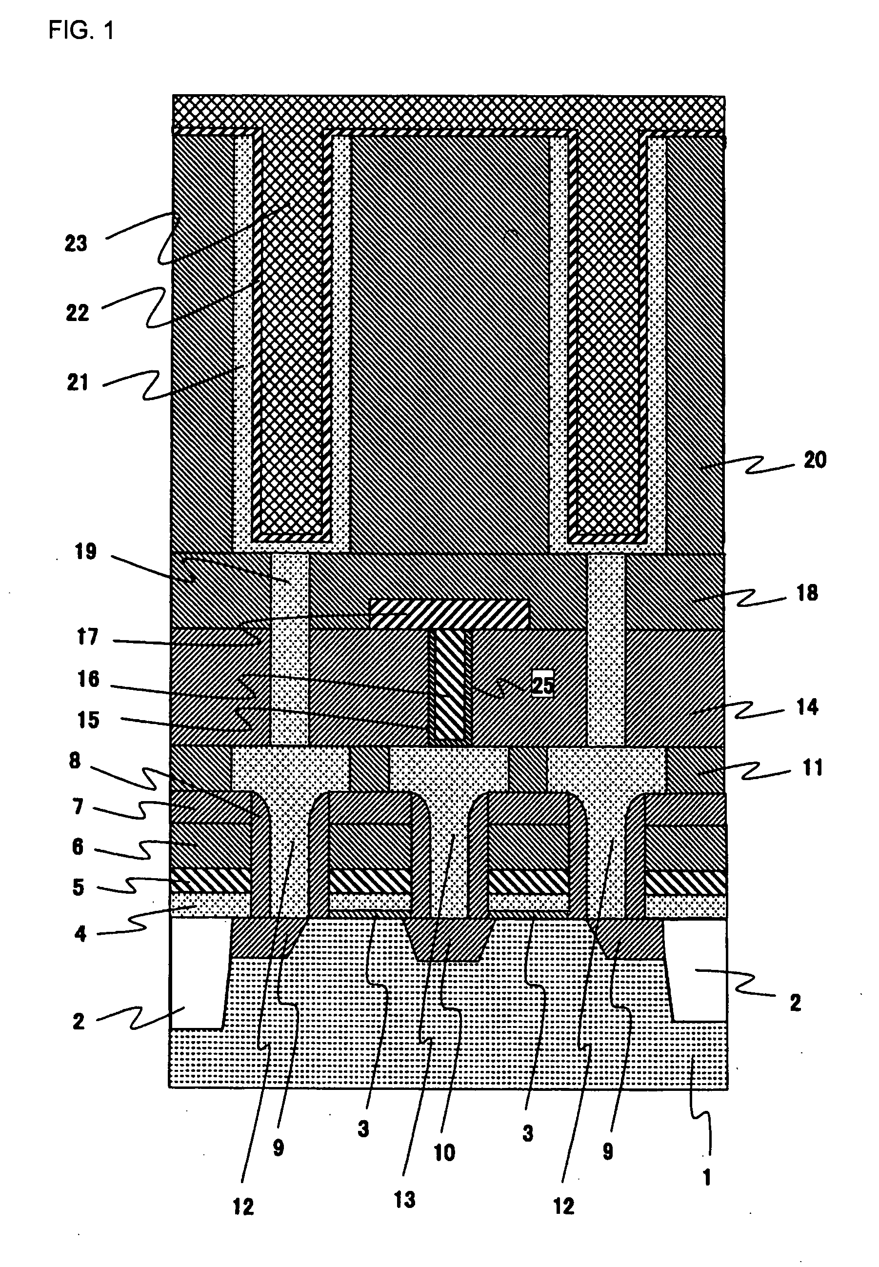
[0043]Firstly, as shown in the memory cell section of FIG. 4A, an element isolation region 2 was formed by a well-known method in prescribed region of a surface of a semiconductor substrate 1 which was made of p-type single-crystal silicon, and then a gate insulating film 3 with a thickness of 4 nm was formed by a thermal oxidation method on the surface of the semiconductor substrate. After that, a first silicon film 4 was grown by a well-known CVD (Chemical Vapor Deposition) method with monosilane (SiH4) being used as a source gas. The thickness of the first silicon film 4 was set to be 70 nm. Next, a metal film 5 was grown to a thickness of 90 nm by a well-known sputtering method, and, further, a silicon nitride film 6 were grown to a thickness of 120 nm by a well-known plasma CVD method with monosilane and ammonia (NH4) being used as source gases, and a silicon oxide film 7 were grown to a thickness of 80 nm by a well-known plasma CVD method with monosilane and dinitrogen monoxid...


PUM


Abstract

An object of the present inventions is to overcome a problem that the presence of a metal film, which is opaque to a visible light, between a lower layer alignment mark and a photoresist prevents the detection of the lower layer alignment mark, to make the pattern formation difficult. In the present inventions, an insulating film is placed beneath the alignment mark in structure; an alignment mark consisting of said multi-layered film comprising an alignment mark layer and the insulating film, which constitutes a stepped part with an increased difference in level, is first formed, inside a mark hole, in a manner of self-alignment; and then the metal film which is the very cause of the above problem is formed thereon. Since the metal film itself has a stepped shape corresponding to the alignment mark, alignment can be made with great accuracy.

Description

BACKGROUND OF THE INVENTION[0001]1. Field of the Invention[0002]The present invention relates to a method of manufacturing a semiconductor device and more particularly to a method of forming an alignment mark used in lithography, which provides the alignment mark possible to be detected even when a metal film or the like, which is opaque to a visible light, is present between a photoresist and a lower layer pattern.[0003]2. Description of the Prior Art[0004]The semiconductor device formed on the semiconductor substrate is, in general, made by repeated steps of forming an interconnection in a multi-layered layer, forming a contact plug to connect an upper interconnection with a lower interconnection, and the like. For instance, in order to connect a lower layer interconnection with an upper layer interconnection which is formed above the lower layer interconnection through an insulating film, the following steps may be taken.[0005]Firstly, after a layer for the lower layer interconne...

Claims


Application Information

Patent Timeline
Patent Type & Authority Applications(United States)
IPC IPC(8): H01L21/8234H01L21/76H01L21/44
CPCG03F9/7076G03F9/708H01L27/10894H01L27/10891G03F9/7084H10B12/488H10B12/09
Inventor SUZUKI, KAZUSHI
Owner LONGITUDE SEMICON S A R L
Why Eureka
Try Eureka