Semiconductor device and manufacturing method thereof

a technology of semiconductor devices and semiconductors, applied in semiconductor devices, semiconductor/solid-state device details, electrical apparatus, etc., can solve the problems of gate parasitic resistance, increased element operation speed, and difficult to achieve ultrafine elements high performance results

Inactive Publication Date: 2007-12-06
KK TOSHIBA
View PDF2 Cites 31 Cited by
  • Summary
  • Abstract
  • Description
  • Claims
  • Application Information

AI Technical Summary

Problems solved by technology

However, in recent years, high performances resulting from ultrafine elements have been difficult to achieve due to various limitations in physical properties.
For example, for a gate electrode using silicon, there have been pointed out the following problems: elicitation of the gate parasitic resistance with an increase in element operation speed, the reduction of the effective insulating film capacitance due to the carrier depletion at the insulating film interface, variations in threshold voltage due to penetration of added impurities into the channel region, and other problems.
In addition, if an insulating film higher in dielectric constant than a silicon oxide film is used for the gate insulating film, even though an impurity is added, an effect of adjusting the work function does not obtained.

Method used


Image

  • Semiconductor device and manufacturing method thereof
  • Semiconductor device and manufacturing method thereof
  • Semiconductor device and manufacturing method thereof

Examples


Embodiment Construction

[0036]Embodiments of the invention will be described with reference to the accompanying drawings.

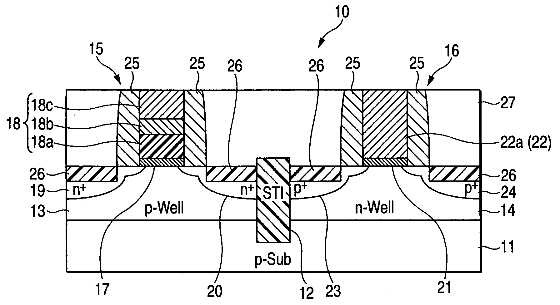
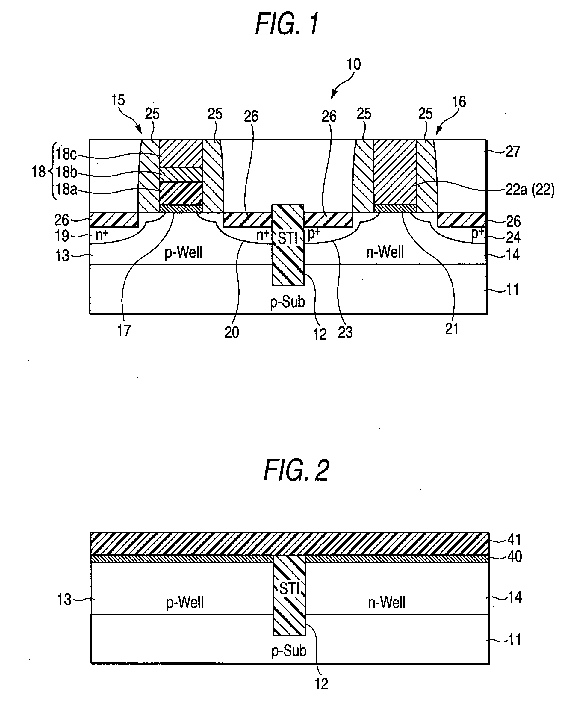
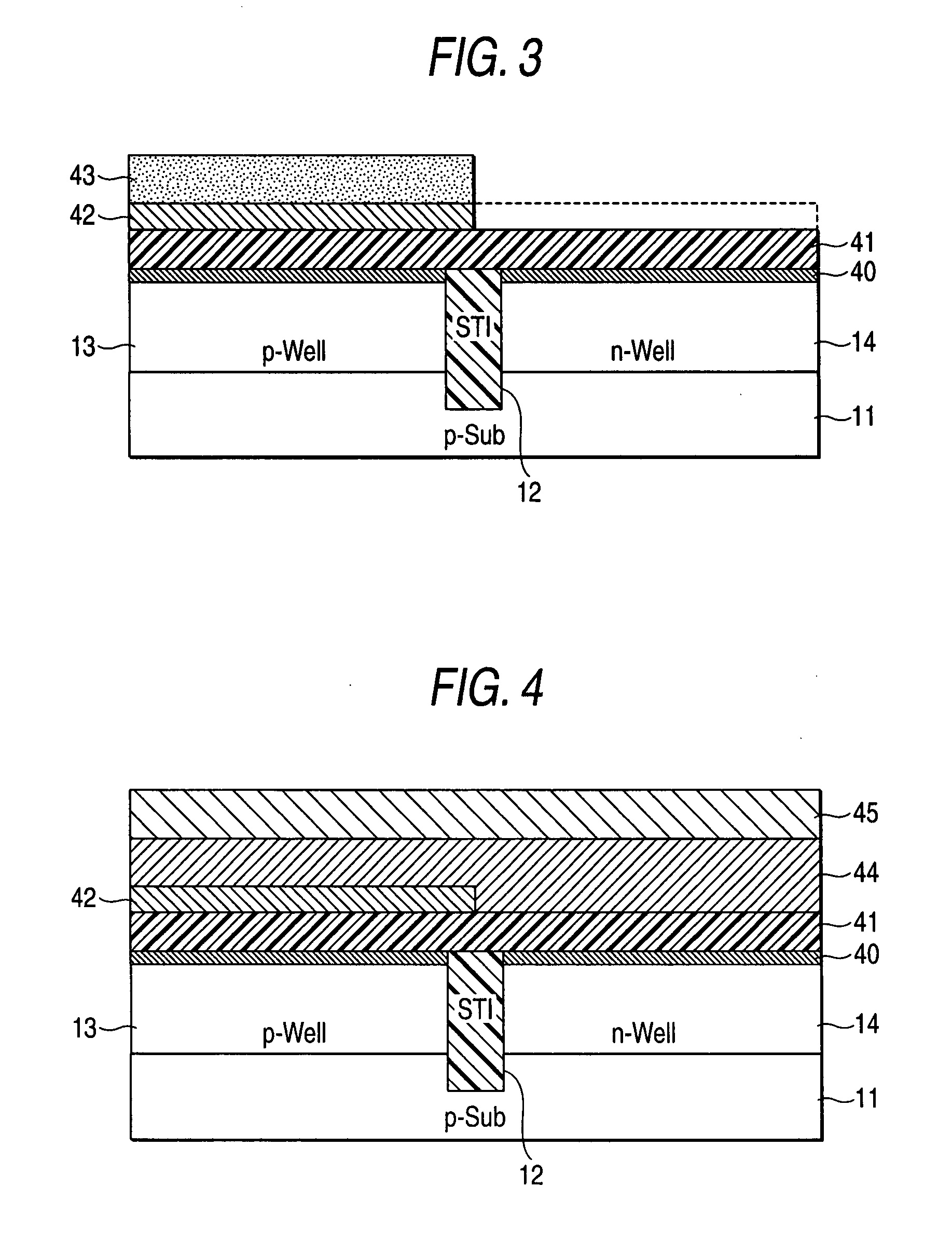
[0037]FIG. 1 is a cross sectional view showing a semiconductor device according to an embodiment of the invention, and FIGS. 2 to 13 are each a cross sectional view showing a manufacturing step of the semiconductor device.

[0038]In this embodiment, a CMOS transistor having an N-channel MOS transistor and a P-channel MOS transistor will be explained as an example of the semiconductor device.

[0039]As shown in FIG. 1, a semiconductor device 10 of this embodiment includes: a P-type well region (P-type semiconductor layer) 13 and an N-type well region (N-type semiconductor layer) 14 which are formed in a semiconductor substrate such as a P-type silicon substrate 11 and insulated and isolated by a STI (Shallow Trench Isolation) 12; an NMOS transistor 15 formed with the P-type well region 13; and a PMOS transistor 16 formed with the N-type well region 14.

[0040]The NMOS transistor 15 includes: a ...


PUM


Abstract

A semiconductor device includes: a P-type semiconductor layer formed in a surface region of a semiconductor substrate; a first gate insulating film formed on the P-type semiconductor layer; a first gate electrode; and a first source region and a first drain region formed in the P-type semiconductor layer to interpose a region under the first gate electrode in a direction of gate length. The first gate electrode includes: a first silicide film formed on the first gate insulating film and containing nickel silicide having a first composition ratio of nickel to silicon as a main component; a conductive film formed on the first silicide film; and a second silicide film formed on the conductive film and containing nickel silicide having a second composition ratio of nickel to silicon as a main component. The second composition ratio is larger than the first composition ratio.

Description

CROSS-REFERENCE TO RELATED APPLICATIONS[0001]This application is based upon and claims the benefit of priority from Japanese Patent Application No. 2006-150562, filed on May 30, 2006, the entire contents of which are incorporated herein by reference.BACKGROUND[0002]1. Field[0003]The present invention relates to a semiconductor device, such as an insulated gate field effect transistor, and a manufacturing method thereof.[0004]2. Description of the Related Art[0005]A silicon very large scale integrated circuit is one of the basic technologies supporting a future highly information-oriented society. In order to achieve a high function integrated circuit, it is necessary to obtain high performances of semiconductor devices, such as a MOSFET (Metal-Oxide-Semiconductor Field Effect Transistor), a CMOSFET (Complementary MOSFET), etc., which are elements of the integrated circuit.[0006]High performances of semiconductor elements have been basically accomplished according to a proportional r...

Claims


Application Information

Patent Timeline
Patent Type & Authority Applications(United States)
IPC IPC(8): H01L29/76H01L21/8238
CPCH01L21/28052H01L21/28097H01L21/823835H01L21/823842H01L27/092H01L2924/0002H01L29/4933H01L29/4975H01L2924/00
Inventor WATANABE, TAKESHI
Owner KK TOSHIBA
Why Eureka
Try Eureka