USB 2.0 Transmitter Using Only 2.5 Volt CMOS Devices

Active Publication Date: 2007-12-06
SYNOPSYS INC
View PDF6 Cites 23 Cited by
  • Summary
  • Abstract
  • Description
  • Claims
  • Application Information

AI Technical Summary

Benefits of technology

[0011]The present invention is directed to a 3.3V output stage for a USB transmitter that avoids subjecting the transistors to potentials greater than 2.5V, even during a 5V short condition, by utilizing a cascode design approach combined with modified pullup/pulldown signal levels, and cascode biasing that matches pullup and pulldown impedance during normal oper

Problems solved by technology

A problem with conventional USB transmitter 10 is that leading edge CMOS fabrication processes (nodes) typically do not support 3.3V devices (i.e., at 65 nm and below the current designs are not portable).
Even in fabrication processes where a 3.3V device is supported, it

Method used


Image

  • USB 2.0 Transmitter Using Only 2.5 Volt CMOS Devices
  • USB 2.0 Transmitter Using Only 2.5 Volt CMOS Devices
  • USB 2.0 Transmitter Using Only 2.5 Volt CMOS Devices

Examples


Example

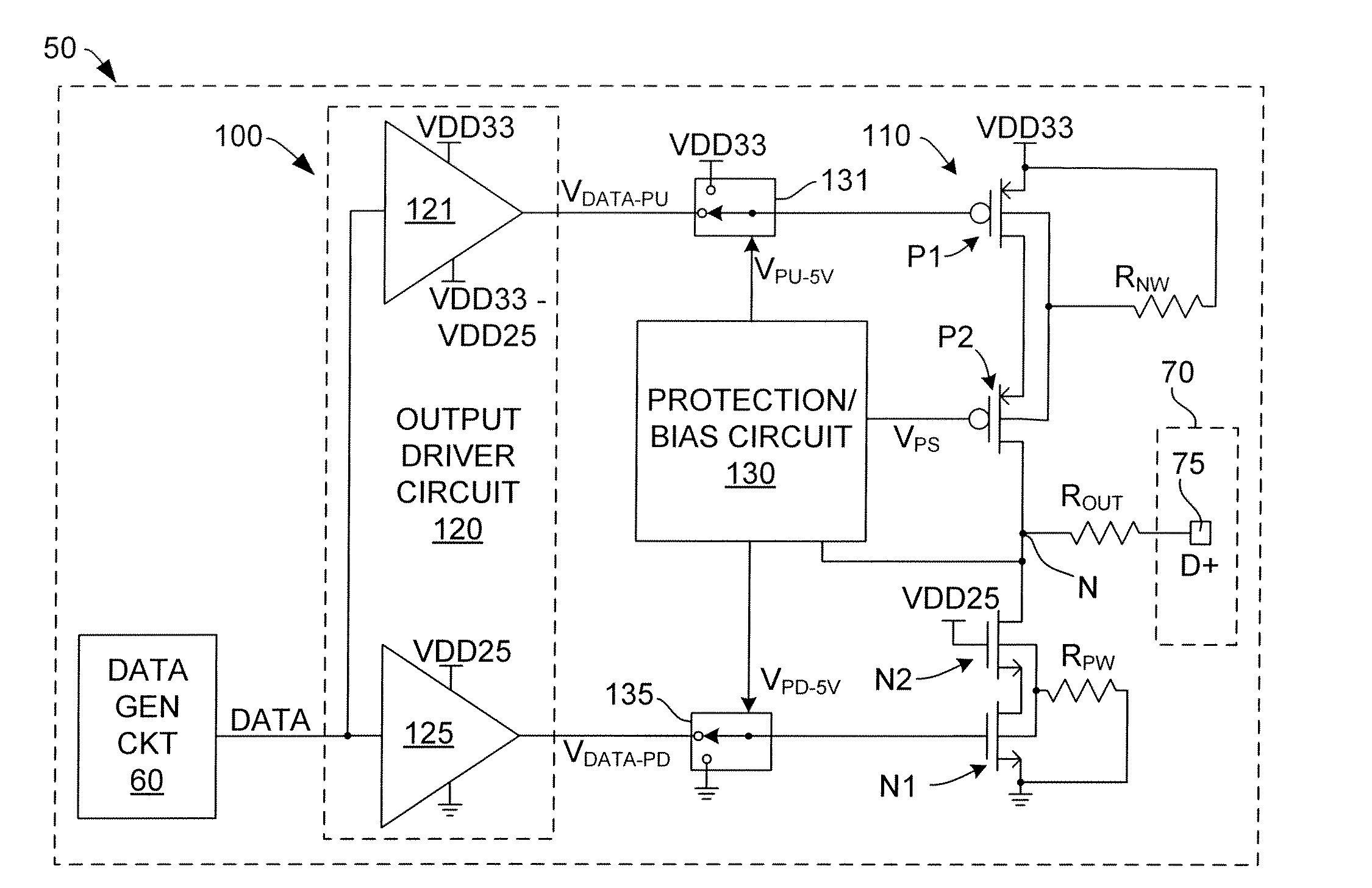
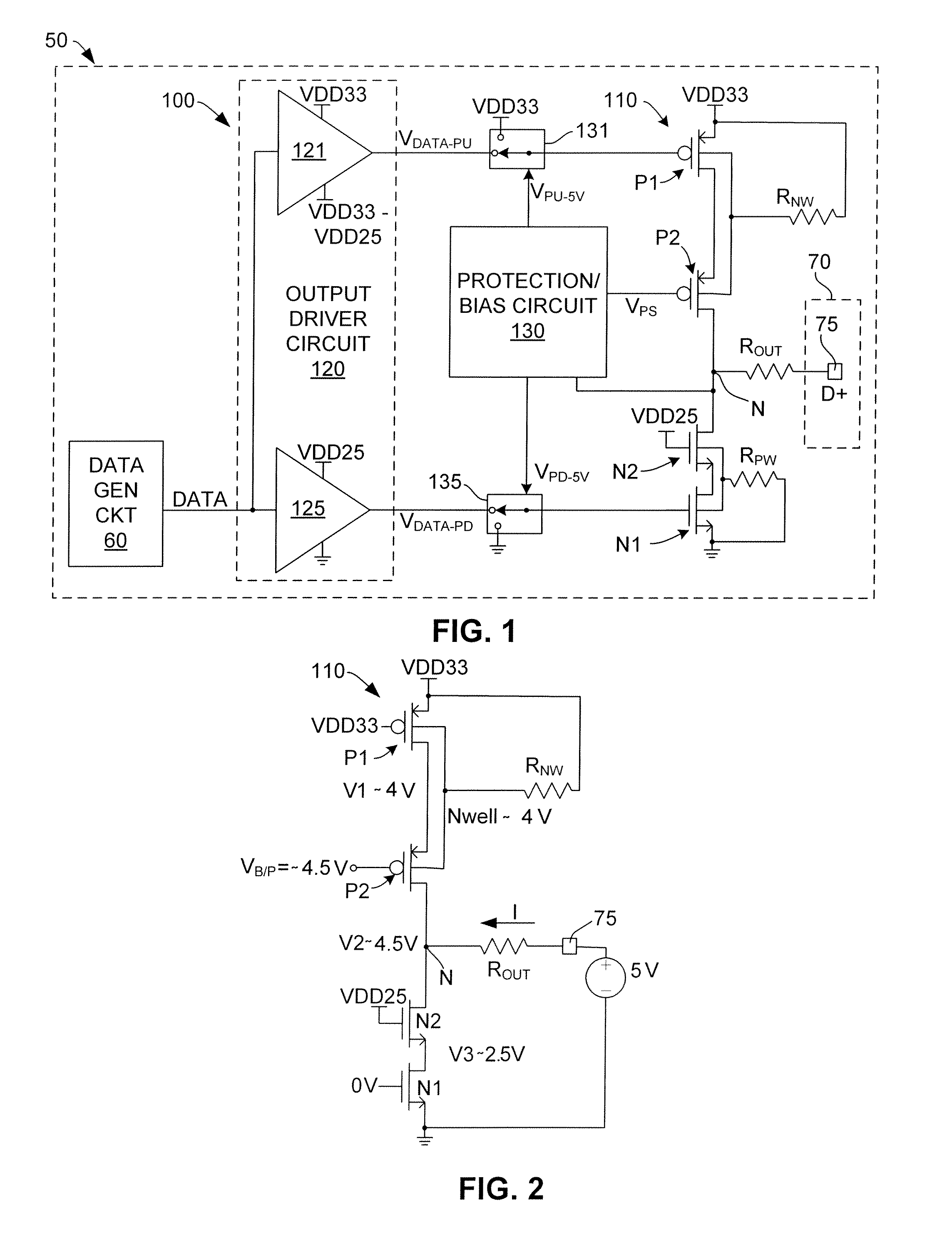
[0020]The present invention relates to an improved USB device (apparatus), and in particular to an improved transmitter output stage for a USB device. The following description is presented to enable one of ordinary skill in the art to make and use the invention as provided in the context of a particular application and its requirements. As used herein, the term “connected” is used herein to describe the connective relationship between associated terminals of two circuit elements of an integrated circuit (IC) in which the two terminals are connected by a low resistance conductor (e.g., a metal via, wire, trace or other structure), and is distinguished from the term “coupled”, which indicates the presence of zero or more passive or active elements disposed in the current path between the associated terminals. In addition the term “2.5V device” is intended to describe a metal-oxide silicon (MOS) type transistor that is fabricated using a conventional CMOS fabrication process having a ...


PUM


Abstract

A USB transmitter 3.3V output stage includes a PMOS cascode transistor connected between a PMOS pullup transistor and a USB port data pin, an NMOS cascode transistor connected between an NMOS pulldown transistor and the data pin, and an output driver circuit that generates a pullup signal range of 0.8V to 3.3V, and a pulldown signal range of 0V to 2.5V, whereby the pullup and pulldown transistors are subjected to 2.5V gate-to-source potentials. A protection/bias circuit biases the PMOS cascode transistor during normal operation such that the pullup resistance matches the pulldown resistance, and turns off the PMOS cascode transistor to shut off the pullup path during a 5V short condition. N-wells of the PMOS pullup and cascode transistors are connected to the 3.3V supply via a resistor.

Description

BACKGROUND OF THE INVENTION[0001]1. Field of the Invention[0002]The invention relates to the field of computer electronics, and in particular, to a system and method for enabling low-power universal serial bus communications.[0003]2. Related Art[0004]The universal serial bus (USB) protocol is a popular communications protocol that allows a wide range of modern electronic devices and peripherals (e.g., scanners, digital cameras, personal digital assistants, and digital music players) to communicate with another peripheral. The present USB 2.0 specification (“Universal Serial Bus Specification”, Revision 2.0, Apr. 27, 2000) defines three signaling levels that can be supported by USB-compliant devices. The three levels include a low-speed mode operating at 1.5 Mbps at 3.3 V, a full-speed mode operating at 12 Mbps at 3.3 V, and a high-speed mode that signals at 480 Mbps at 400 mV.[0005]Modern high-speed USB 2.0-compliant devices include USB transmitters having 3.3V output drivers. For e...

Claims


Application Information

Patent Timeline
IPC IPC(8): H03K19/094
CPCH03K19/00315
Inventor CHONG, EUHANTOFFOLON, DINO A.
Owner SYNOPSYS INC
Why Eureka
Try Eureka