Chip capacitor

a chip capacitor and capacitor body technology, applied in capacitors, capacitor housing/encapsulation, electrical devices, etc., can solve the problems of reducing the bonding area of ag paste 124/b>, hampering stable electrical connection, etc., to ensure structural stability, reduce external moisture infiltration, and increase strength

Inactive Publication Date: 2007-12-06
SAMSUNG ELECTRO MECHANICS CO LTD
View PDF8 Cites 32 Cited by
  • Summary
  • Abstract
  • Description
  • Claims
  • Application Information

AI Technical Summary

Benefits of technology

[0019]The present invention has been made to solve the foregoing problems of the prior art and therefore an aspect of the present invention is to provide a chip capacitor in which anode and cathode leads are bonded together with greater strength to a molding to ensure structural stability as well as minimize infiltration of external moisture to greatly improve moisture resistant characteristics.

Problems solved by technology

Moreover, when the cathode lead 114 is electrically connected to the capacitor device 104 through an Ag paste 124, the Ag paste 124 is decreased in its bonding area, thereby hampering stable electrical connection.

Method used


Image

  • Chip capacitor
  • Chip capacitor
  • Chip capacitor

Examples


Embodiment Construction

[0032]Exemplary embodiments of the present invention will now be described in detail with reference to the accompanying drawings.

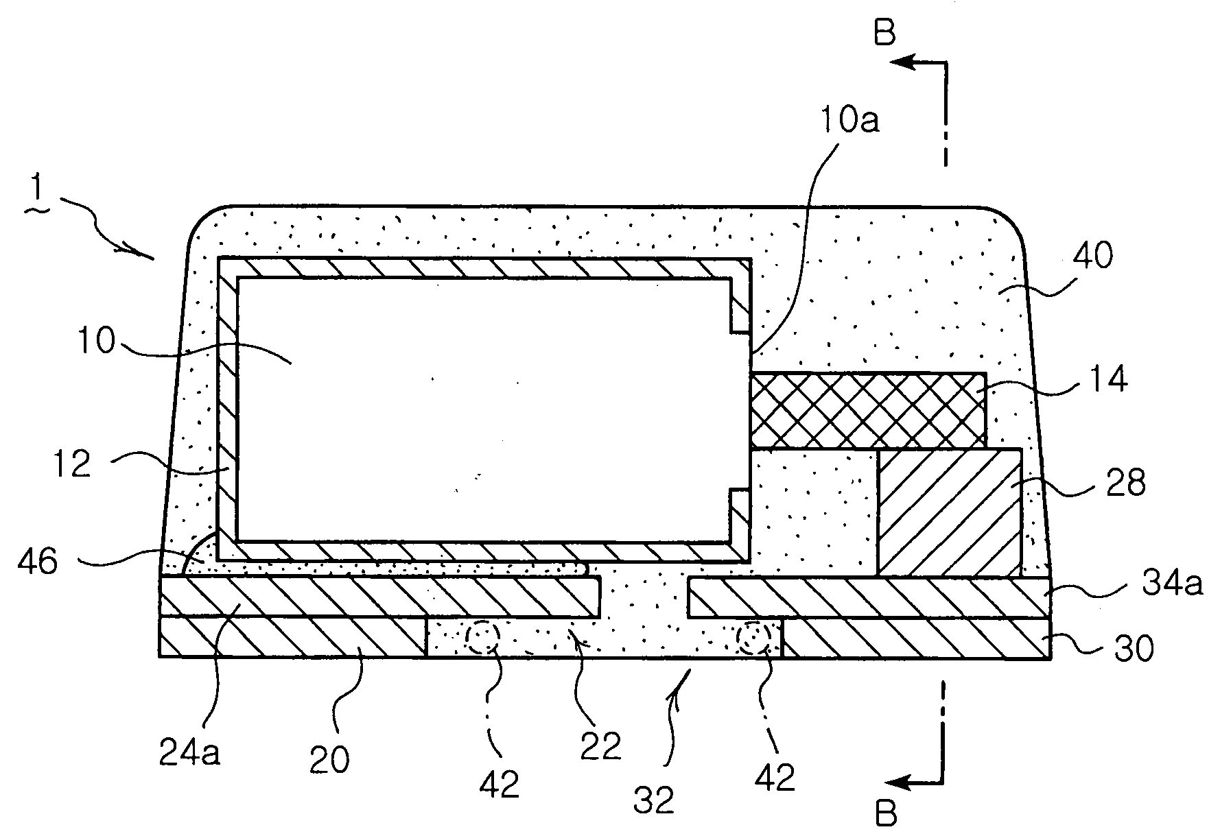
[0033]As shown in FIGS. 3 and 4, a chip capacitor 1 according to the invention includes a capacitor device 10 having a cathode layer 12 formed on an outer surface thereof and an anode wire 14 protruding from a portion thereof.

[0034]The capacitor device 10 is a dielectric device obtained by compressing a tantalum oxide (Ta2O5) powder into a parallelepiped shape. But the invention is not limited to tantalum Ta, and optionally, other material such as Nibio (Nb) can be employed.

[0035]The capacitor device 10 as described above is rectangular box shaped. The capacitor device 10 has a front surface 10a from a portion of which the anode wire 14 is protruded and a rear surface 10b opposing the front surface 10a.

[0036]The capacitor device 10 has a cathode layer 12 formed on an outer surface thereof and a cathode lead 20 electrically connected to the cathode layer 1...


PUM


Abstract

A chip capacitor which can be miniaturized with structural stability. In the chip capacitor, a capacitor device has a cathode layer formed on an outer surface thereof and an anode wire is protruded from a portion thereof. A cathode lead is electrically connected to the cathode layer. An anode lead is electrically connected to the anode wire through a weld reinforcement. A molding is configured to cover the capacitor device in such a way that the cathode and anode leads are only partially exposed. Protrusions are protruded from outer surfaces of the cathode and anode leads, respectively, thereby forming steps on the outer surfaces thereof. In the chip capacitor, the leads and molding are bonded with much greater strength, thus more structurally robust. Also, this prevents external moisture from penetrating inside the chip capacitor, thereby significantly enhancing moisture resistance.

Description

CLAIM OF PRIORITY[0001]This application claims the benefit of Korean Patent Application No. 2006-49779 filed on Jun. 2, 2006 in the Korean Intellectual Property Office, the disclosure of which is incorporated herein by reference.BACKGROUND OF THE INVENTION[0002]1. Field of the Invention[0003]The present invention relates to a chip capacitor miniaturizable with structural stability, more particularly, in which steps are formed on outer surfaces of anode and cathode leads, respectively, to bond a molding and the leads together with greater strength, and external moisture is minimally penetrated thereinto to assure stable electrical capability.[0004]2. Description of the Related Art[0005]In general, a tantalum capacitor, i.e., a solid chip capacitor is widely used in general industrial devices and application circuits requiring a low range of rated voltage. Especially, the solid chip capacitor is broadly utilized in circuits with poor frequency characteristics. Also, the solid chip cap...

Claims


Application Information

Patent Timeline
Patent Type & Authority Applications(United States)
IPC IPC(8): H01G9/00H01G4/228
CPCH01G9/08H01G9/012H01G9/00
Inventor KIM, JAE KWANGMYUNG, HEE DONGPARK, JAE JUNLEE, GYU HWANG
Owner SAMSUNG ELECTRO MECHANICS CO LTD
Why Eureka
Try Eureka