Solid state light emitting device and method of making same

Active Publication Date: 2007-12-06
CREELED INC
View PDF6 Cites 280 Cited by
  • Summary
  • Abstract
  • Description
  • Claims
  • Application Information

AI Technical Summary

Benefits of technology

[0028] In accordance with the present invention, it has been found that by providing a first element which has at least a first region which has an index of refraction gradient (in some cases, a stepped index of refraction gradient, and in some cases a substantially continuous index of refraction gradient), better light extraction efficiency from the light emitting active layer structure can be obtained.
[0029] While not being bound by any theory, it is believed that the reason the first aspect of the present invention (as well as the other aspects of the present invention, described below) achieves improved light extraction efficiency is by reducing the amo

Problems solved by technology

It is well-known that incandescent light bulbs are very energy-inefficient light sources—about ninety percent of the electricity they consume is released as heat rather than light.
Fluorescent light bulbs are more efficient than incandescent light bulbs (by a factor of about 10) but are still less efficient as compared to solid state light emitters, such as light emitting diodes.
In addition, as compared to the normal lifetimes of solid state light emitters, e.g., light emitting diodes, incandescent light bulbs have relatively short lifetimes, i.e., typically about 750-1000 hours.
Fluorescent bulbs have longer lifetimes (e.g., 10,000-20,000 hours) than incandescent lights, but provide less favorable color reproduction.
Another issue faced by conventional light fixtures is the need to

Method used


Image

  • Solid state light emitting device and method of making same
  • Solid state light emitting device and method of making same
  • Solid state light emitting device and method of making same

Examples


first embodiment

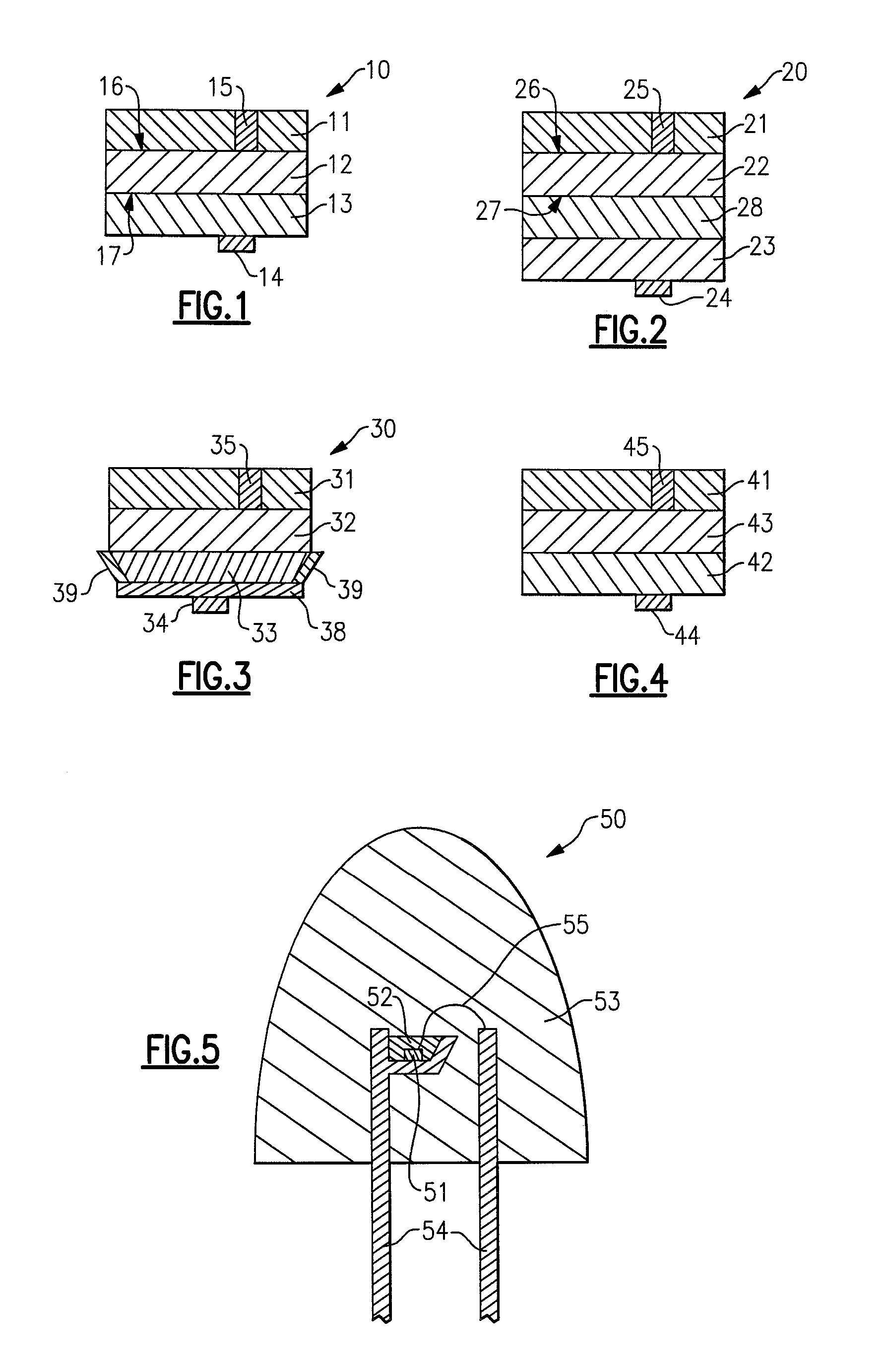
[0132]FIG. 1 is a schematic cross-sectional illustration of a first embodiment according to the present invention. Referring to FIG. 1, there is shown a light emitter 10 including a first element 11, a light emitting active layer structure 12, a second element 13, a contact 14 and a metallized contact 15. The first element 11, the light emitting active layer structure 12, and the second element 13 are each generally rectilinear, i.e., a top view of any of them would show a generally rectangular perimeter.

[0133] In this embodiment, the first element is in direct contact with the light emitting active layer structure.

[0134] In this embodiment, the light emitting active layer structure has an active layer structure first side 16 and an active layer structure second side 17. The first element 11 is positioned on (and in direct contact with) the active layer structure first side 16, and the active layer second side 17 is positioned on (and in direct contact with) the second element 13. ...

second embodiment

[0135]FIG. 2 is a schematic cross-sectional illustration of a second embodiment according to the present invention. Referring to FIG. 2, there is shown a light emitter 20 including a first element 21, a light emitting active layer structure 22, a reflective element 28, a second element 23, an electrically conductive contact 24 and an electrically conductive contact 25.

[0136] In this embodiment, the first element is in direct contact with the light emitting active layer structure.

[0137] In this embodiment, the light emitting active layer structure has an active layer structure first side 26 and an active layer structure second side 27. To illustrate the terminology described above, the first element 21 is positioned on (and in direct contact with) the active layer structure first side 26 (and vice-versa), the active layer second side 27 is positioned on (but not in direct contact with) the second element 23 (and vice-versa), the reflective layer 28 is positioned on (and in direct co...

third embodiment

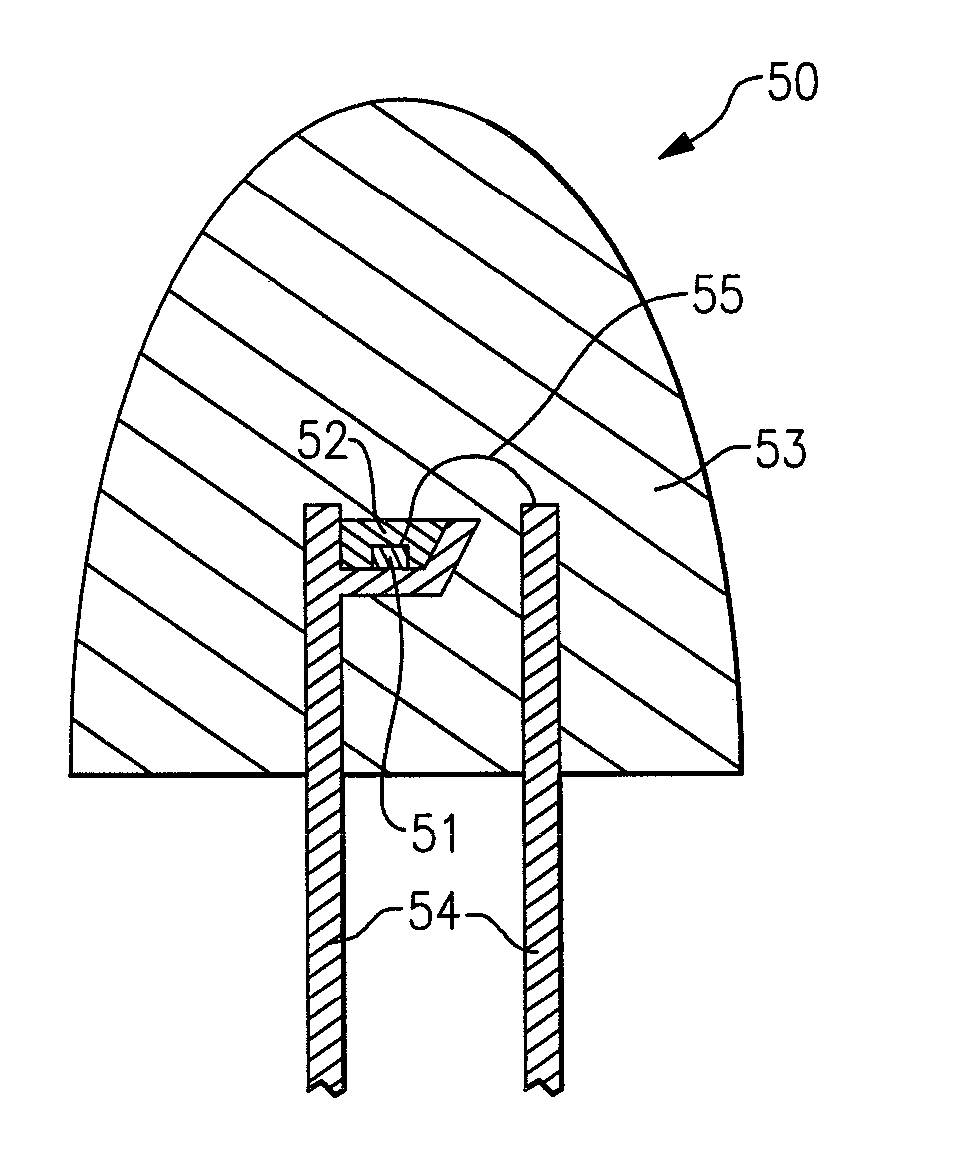
[0138]FIG. 3 is a schematic cross-sectional illustration of a third embodiment according to the present invention. Referring to FIG. 3, there is shown a light emitter 30 including a first element 31, a light emitting active layer structure 32, a second element 33, a first reflective layer 38, a second reflective layer 39, an electrically conductive contact 34 and an electrically conductive contact 35. The second reflective layer 39 goes around the entire circumference of the second element 33. The angle of the beveled second reflective layer 39, relative to a vertical (in the orientation shown in FIG. 3) line is preferably not larger than 45 degrees. In this embodiment, one method of providing the beveled mirrors is to perform partial cuts in the wafer to provide beveled grooves, then metallize the grooves, and then complete the cutting (i.e., to divide the wafer into a plurality of dice).


PUM


Abstract

There is provided a solid state light emitting device comprising at least one light emitting active layer structure and at least one structure selected from among: (1) a first element having at least a first region which has an index of refraction gradient, (2) a first element, at least a portion of which has an index of refraction which is lower than an index of refraction of a side of the active layer, (3) first and second elements, in which one side of the second element is positioned on a side of the active layer and the first element is positioned on the other side of the second element, and in which at least a portion of the first element has an index of refraction which is lower than the index of refraction of at least a portion of the second element. Also provided are methods of making such devices.

Description

CROSS-REFERENCE TO RELATED APPLICATIONS [0001] This application claims the benefit of U.S. Provisional Patent Application No. 60 / 808,925, filed May 26, 2006, the entirety of which is incorporated herein by reference.FEILD OF THE INVENTION [0002] The present invention relates to a solid state light emitting device. More particularly, the present invention relates to a solid state light emitting device with improved light extraction efficiency. The present invention also relates to a method of making such solid state light emitting devices. BACKGROUND OF THE INVENTION [0003] A large proportion (some estimates are as high as twenty-five percent) of the electricity generated in the United States each year goes to lighting. Accordingly, there is an ongoing need to provide lighting which is more energy-efficient. It is well-known that incandescent light bulbs are very energy-inefficient light sources—about ninety percent of the electricity they consume is released as heat rather than ligh...

Claims


Application Information

Patent Timeline
IPC IPC(8): G02B6/10H01L33/38H01L33/44H01L33/54
CPCH01L33/38H01L33/44H01L33/54H01L2224/48091H01L2224/8592H01L2224/48247H01L2924/00014
Inventor NEGLEY, GERALD H.HUNTER, F. NEAL
Owner CREELED INC
Why Eureka
Try Eureka