Semiconductor cutting device, semiconductor cutting method, semiconductor cutting system, laser cutting device and laser cutting method

a cutting device and semiconductor technology, applied in the direction of metal working equipment, printed circuit manufacturing, manufacturing tools, etc., can solve the problems of deteriorating scanning position accuracy of laser beams, increasing the size of laser oscillators and high cost, and reducing so as to reduce the cutting section inclination

Inactive Publication Date: 2007-12-13
APIC YAMADA CORP
View PDF11 Cites 16 Cited by
  • Summary
  • Abstract
  • Description
  • Claims
  • Application Information

AI Technical Summary

Benefits of technology

[0022]The present invention provides a semiconductor cutting apparatus capable of reducing an inclination of a cutting section by a laser beam of a semiconductor substrate without extending the distance from the semiconductor substrate to a laser scanning center.
[0023]Further, the present invention provides a semiconductor device cutting system capable of performing cutting of a semiconductor device including an odd-shaped line portion from the semiconductor substrate at a high speed, and moreover, securing a high grade cutting section.
[0024]Further, the present invention provides a semiconductor cutting apparatus capable of securing a high grade cutting section by cutting a semiconductor substrate with a laser beam and suppressing an increase in cutting width, and moreover, performing the cutting at a high speed, while preventing changes in the nature of the semiconductor.

Problems solved by technology

However, when the scanning center is away from the semiconductor substrate, the necessity of increasing the laser output arises, and the scanning position accuracy of the laser beam is deteriorated.
The increase in the laser output leads to the increase in the size of a laser oscillator and the high cost.
Further, when the scanning position accuracy is deteriorated, the cut section becomes coarse, and the size management of the semiconductor device to be cut out becomes difficult.
However, the method of using the water jet, as compared to the method of using the cutting blade, is slow in cutting speed.
However, when the strength of the laser beam is set high, the semiconductor may change its nature.
Further, when an attempt is made to complete the cutting by the laser beam irradiation in a single time, the cutting section becomes coarse.
However, when all the predetermined cutting lines (entire periphery of the semiconductor device) are cut by this method, the cutting processing speed often becomes slow.
However, when an attempt is made to complete the cutting by the laser beam scan in a single time, the cutting section becomes coarse.
Further, in this case, even when the output of the laser beam is high, it is necessary to make the cutting (scan) speed slow to some extent.
However, in this method, the coarseness of the cutting sections of the other layers becomes worse than expected and the increase in the cutting width of other layers due to heat becomes noticeable.
However, when the laser receiving member is provided with the damping structure or the scattering reflection structure of the laser beam as disclosed in Japanese Patent Laid-Open No. 10-328875, the structure of the laser receiving member becomes complicated, which leads to the increase in the size of laser receiving member and high cost.
However, in the conventional laser cutting apparatus, the soot and dust not removable enough by the dust collection air are adhered to the workpiece and the laser receiving member, thereby necessitating frequent cleaning.
However, when an amount of the processing debris generated from the workpiece is great and the adhering amount thereof is also great, there are often the cases where the cleaning after the cutting processing takes long time and the processing debris not removable by the cleaning is left remain.
Consequently, cleaning after the cutting processing must be performed at both surfaces of the workpiece, and there is a possibility that this becomes disadvantageous in time and the remaining amount of the processing debris increases.
Further, though the laser beam is emitted from the light emission surface (lens surface) of the laser oscillator toward the workpiece, when the processing debris generated from the workpiece adheres to the light emission surface, an appropriate laser irradiation is unable to be performed.

Method used


Image

  • Semiconductor cutting device, semiconductor cutting method, semiconductor cutting system, laser cutting device and laser cutting method
  • Semiconductor cutting device, semiconductor cutting method, semiconductor cutting system, laser cutting device and laser cutting method
  • Semiconductor cutting device, semiconductor cutting method, semiconductor cutting system, laser cutting device and laser cutting method

Examples


first embodiment

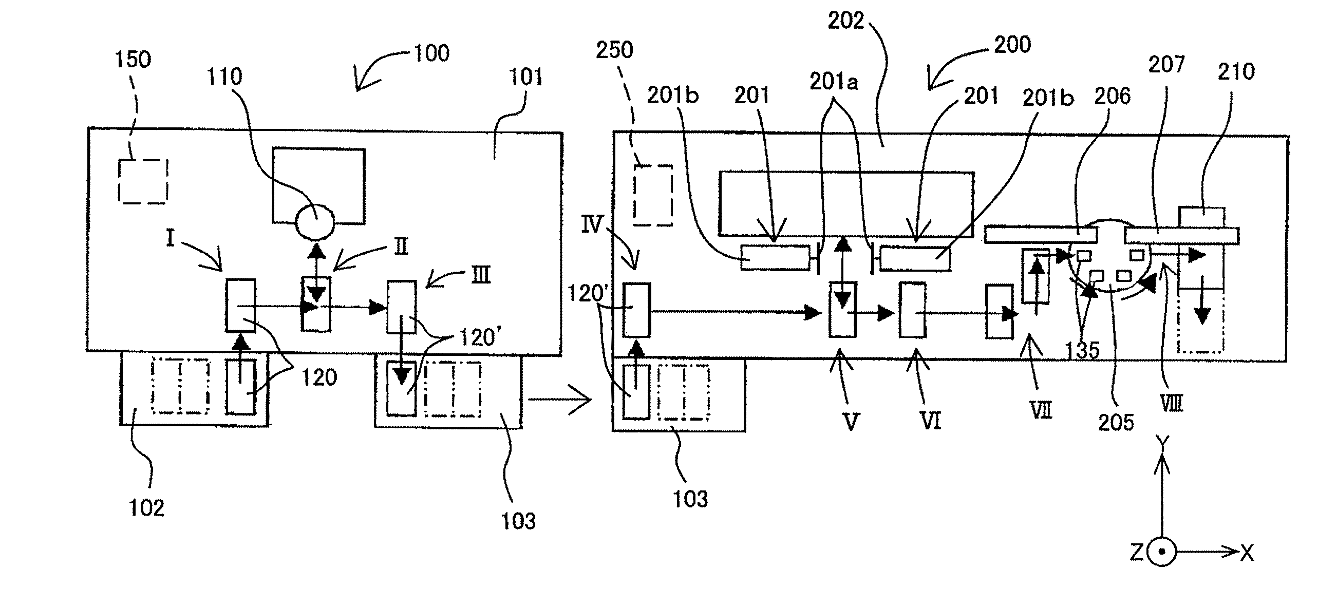
[0076]FIG. 1 shows the configuration of a semiconductor cutting system seen from the above, which is a first embodiment of the present invention. In FIG. 1, reference numeral 100 denotes a laser cutting part constituted by a laser cutting processing apparatus, and reference numeral 200 denotes a blade cutting part constituted by a dicing apparatus.

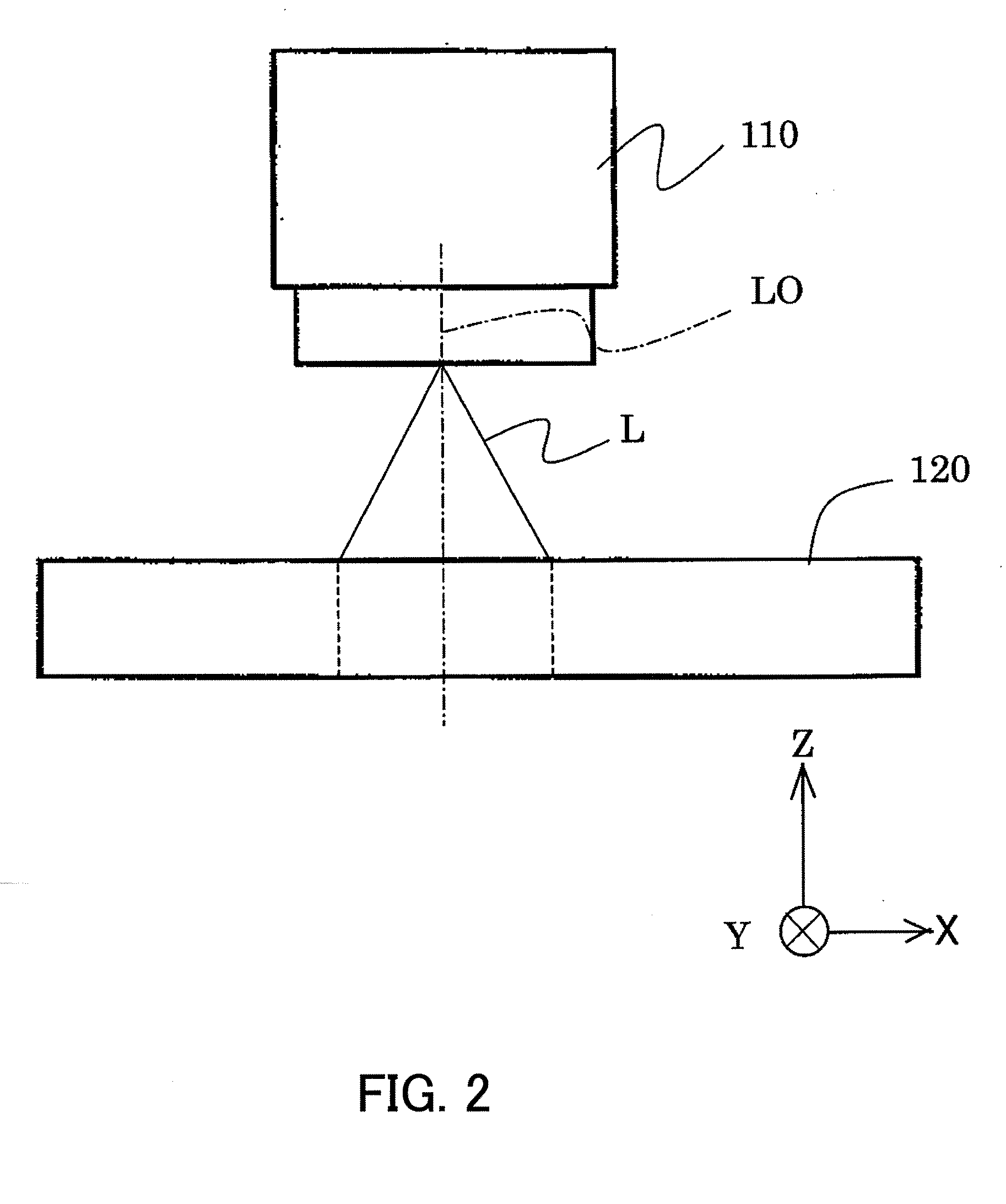
[0077]The laser cutting part 100 includes a base 101 and a laser oscillator 110 installed on the base 101. Reference numeral 102 denotes a first substrate magazine with large quantities of semiconductor substrates 120 before laser cutting processing stored therein, and by an unshown first transport mechanism, the semiconductor substrates 120 are transported to a first position I on the base 101 from the first substrate magazine 102 one by one.

[0078]The semiconductor substrate 120 before the cutting processing is shown in FIG. 5. Here, as one of the semiconductor substrates 120, the memory card substrate is shown as an example. The memory c...

second embodiment

[0140]FIG. 21 shows the configuration of a semiconductor cutting system which is a second embodiment of the present invention. The system of the first embodiment (FIG. 1) has been described on the case where the laser cutting part 100 and the blade cutting part 200 are combined into a separate apparatus. However, in the present embodiment, the system is configured to be one apparatus having both of the laser cutting part 100 and the blade cutting part 200.

[0141]In FIG. 21, the components common with the first embodiment (FIG. 1) are attached with the same reference numerals as the first embodiment, and this will be substituted for the description thereof.

[0142]In the present embodiment, a laser oscillator 10 and two cutting blade units 201 are provided on a base 101.

[0143]The method and procedure for cutting a substrate in the present embodiment are the same as the first embodiment.

third embodiment

[0144]FIG. 22 shows the configuration of a semiconductor cutting system which is a third embodiment of present invention. In the systems shown in the first embodiment (FIG. 1) and the second embodiment (FIG. 21), after the cutting of the corner portions by the laser cutting part 100, the cutting of the straight line portions by the blade cutting part 200 is performed. In contrast to this, in the present embodiment, first, the straight line portions are cut by a blade cutting part 200, and then, the corner portions of the individualized memory card region are cut by a laser cutting part 100.

[0145]In FIG. 22, the components common with the first and second embodiments are attached with the same reference numerals as these embodiments, and this will be substituted for the description. Further, in the present embodiment, though a case is shown where the system is configured to be one apparatus provided with two blade cutting units 201 and a laser oscillator 10 on a base 101, similarly t...


PUM

PropertyMeasurementUnit
angleaaaaaaaaaa
Q switch frequencyaaaaaaaaaa

Abstract

A semiconductor cutting apparatus is disclosed which is capable of reducing an inclination of a cutting section by a laser beam of a semiconductor substrate without extending the distance from the semiconductor substrate to a laser scanning center. The apparatus includes a laser oscillator, a transport mechanism causing a semiconductor substrate and the laser oscillator to relatively move, and a controller controlling the laser oscillator and the transport mechanism. When a plurality of semiconductor device regions each being surrounded by a predetermined cutting line are provided in the semiconductor substrate, the controller controls the transport mechanism such that a scanning center of the laser beam of the laser oscillator is located above a position inner than the predetermined cutting line of each semiconductor device region and causes the laser oscillator to perform the scanning of the laser beam along the predetermined cutting line of the semiconductor device region.

Description

[0001]This application claims the right of priority under 35 U.S.C. §119 based on Japanese Patent Applications Nos. 2006-160320, filed on Jun. 8, 2006, 2006-160321, filed on Jun. 8, 2006, 2006-160322, filed on Jun. 8, 2006, 2006-197473, filed on Jul. 19, 2006, and 2006-201596, filed on Jul. 25, 2006, and each of which is hereby incorporated by reference herein in its entirety as if fully set forth herein.BACKGROUND OF THE INVENTION[0002]The present invention relates to a cutting apparatus which cut out a workpiece such as an IC chip and a memory card from a semiconductor substrate.[0003]As a method of cutting a semiconductor substrate formed with a plurality of semiconductor device region such as a BGA (ball grid array) and a CSP (chip size package) along a predetermined cutting line so that individual semiconductor device is cut out, Japanese Patent Laid-Open No. 2005-142303 and Japanese Patent Laid-Open No. 2005-238246 disclose a cutting method using a laser beam.[0004]In the cutt...

Claims


Application Information

Patent Timeline
Patent Type & Authority Applications(United States)
IPC IPC(8): B23K26/38B23K26/14
CPCB23K26/04B23K26/0807B23K2201/40H05K2203/1476H05K3/0008H05K3/0032H05K3/0052H05K1/0366B23K26/082B23K2101/40
Inventor ANDO, SYUJIUCHIYAMA, SHIGEYUKIOGUCHI, TATSUSHI
Owner APIC YAMADA CORP
Why Eureka
Try Eureka