
Mounting integrated circuit dies for high frequency signal isolation

Inactive Publication Date: 2007-12-13
PSEMI CORP
View PDF3 Cites 16 Cited by
  • Summary
  • Abstract
  • Description
  • Claims
  • Application Information

AI Technical Summary

Benefits of technology

[0010]A method of configuring connections between a signal switching integrated circuit (IC) die and external circuit terminals is also disclosed. The signal lines include a first signal line, a first signal termination return line, an isolation-target signal line, and an isolation-target termination return line. The method enhances isolation between the first signal line and the isolation-target signal line at a particular frequency when the first signal line is terminated by a terminating impedance coupled between the first signal line and a corresponding termination current return connection. For each of the first signal line and the isolation-target signal line, this method includes splitting the return termination current so that it is conducted via a plurality of return current paths that are established adjacent to and on opposite sides of a path connecting the corresponding signal line between the IC die and the external terminal. The method further includes adjusting capacitive coupling between the first signal line and the isolation target signal line in accordance with any technique as described in more detail below; and adjusting magnetic coupling between the first signal connection and the isolation target signal connection in accordance with any technique described in more detail below, such that the mutual capacitive and magnetic couplings interact to provide an isolation between the signal lines that is higher, at a target frequency subject to stringent isolation requirements, than would be due to either the mutual capacitive coupling alone or the mutual magnetic coupling alone at such target frequency. Each method set forth hereinbelow for changing mutual capacitive coupling between the signal lines, and each method set forth for changing mutual magnetic coupling between the signal lines, and each functional combination of such method, is combined with the configuring method set forth above to create a different embodiment of this method.

Problems solved by technology

An integrated circuit (IC) alone might satisfy such isolation requirements, yet fail when packaged in a carrier.
Techniques by which the IC is protected and connected to the carrier may impair the inherent signal isolation provided by the IC alone.

Method used


Image

  • Mounting integrated circuit dies for high frequency signal isolation
  • Mounting integrated circuit dies for high frequency signal isolation
  • Mounting integrated circuit dies for high frequency signal isolation

Examples


Embodiment Construction

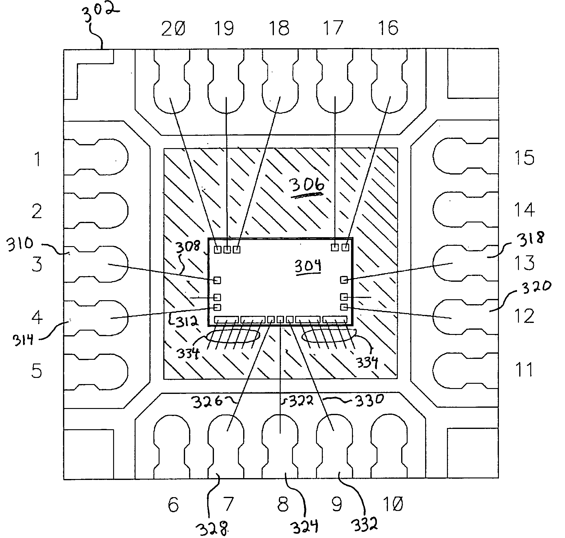
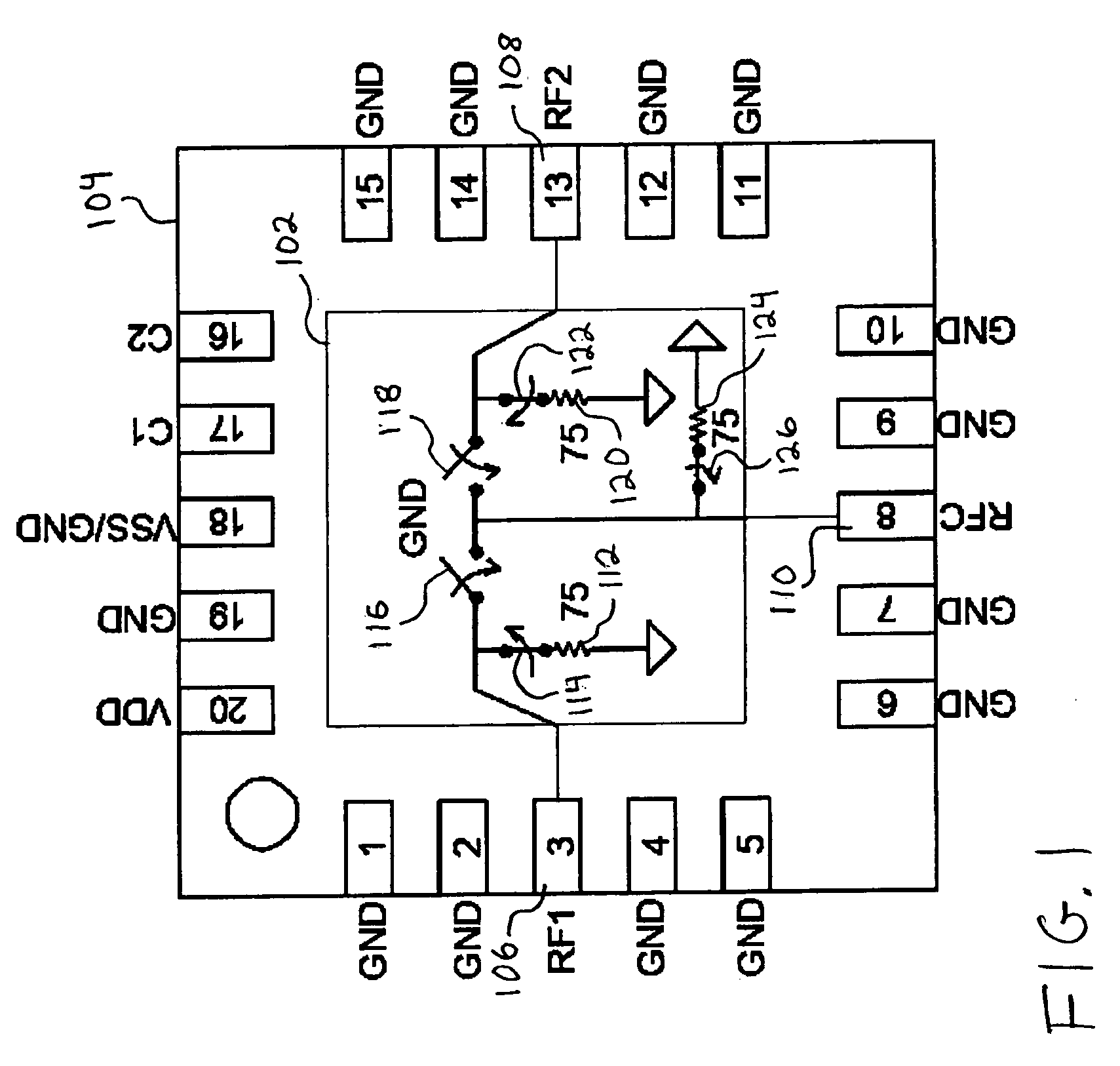
[0020]FIG. 1 illustrates, in a simplified quasi-schematic manner, signal switching functionality for an exemplary integrated circuit (IC) die 102 that is mounted on an IC package or carrier 104. The carrier 104 includes terminals used for connecting the IC to a circuit in which it is employed. In particular, a first RF signal will be connected to a terminal 106 that is labeled “RF1” and indicated as pin “3.” A second RF signal will be connected to a terminal 108 (RF2, 13). An RF common will be connected to a terminal 110 (RFC, 8).

[0021]Each of the RF signal terminals is connected to the IC die 102, which includes switches to connect the signal to either an RF common, or to a termination path. The first RF signal, for example, is typically coupled to a terminating impedance 112 (here, 75 ohms resistive) via a first signal termination switch 114 when a first signal switch 116 is open (so that the signal is not terminated by another circuit). The second RF signal is shown similarly dis...


PUM


Abstract

A method of connecting signal lines between an integrated circuit (IC) die and a carrier or external circuit, and corresponding apparatus. Techniques for adjusting magnetic coupling between terminated signal lines include splitting a return path for termination current and disposing one nearby on either side of the terminated signal line, creating two small termination current loops conducting in opposite directions; using separate terminating impedances, which may be unequal, to control current in each of the loops; and arranging major axes of the termination current loops for a signal to be perpendicular to those of the isolation-target signal. Capacitive coupling adjustments include routing ground potential termination current return connections nearby the signal connection to shield it from the isolated signal line, using dual overlapping connections to shield each return path, and adjusting dielectric material proximity to the signal paths. For isolation across a limited frequency range, increasing either inductive or capacitive mutual coupling above the achievable minimum may create an isolation null at the desired frequency that effects higher isolation than is obtainable with minimum coupling values.

Description

CROSS REFERENCE TO RELATED APPLICATIONS[0001]This application claims the benefit under 35 USC 119 of U.S. Provisional Application identified by attorney docket number PER-017-PROV, Application Ser. No. 60 / 812,191 filed Jun. 9, 2006 and entitled “Mounting Integrated Circuit Dies for High Frequency Signal Isolation” which is hereby incorporated herein in its entirety by reference.BACKGROUND OF THE INVENTION[0002]1. Field of the Invention[0003]The disclosed methods and apparatus relate broadly to electronic integrated circuits (“ICs”), and more specifically to interfacing IC dies to circuits in which they are employed.[0004]2. Related Art[0005]ICs must generally be connected to external circuitry to be useful, and the interconnection itself may impact the net high frequency performance of the IC. For example, FIG. 1 illustrates an exemplary SPDT analog switching circuit. A first high frequency signal, RF1, is input to pin 3. A second high frequency signal, RF2, is input to pin 13. Cont...

Claims


Application Information

Patent Timeline
IPC IPC(8): H01L23/52
CPCH01L23/66H01L2224/0603H01L24/49H01L2223/6611H01L2224/05553H01L2224/05599H01L2224/48247H01L2224/48257H01L2224/49111H01L2224/49171H01L2224/49175H01L2224/85399H01L2924/01005H01L2924/01082H01L2924/14H01L2924/19107H01L2924/30105H01L2924/30107H01L2924/3011H01L2924/3025H01L24/06H01L2224/05554H01L2924/01033H01L2924/01006H01L2924/00014H01L24/48H01L2924/00H01L2224/45099
Inventor ENGLEKIRK, ROBERT MARK
Owner PSEMI CORP
Features
  • Generate Ideas
  • Intellectual Property
  • Life Sciences
  • Materials
  • Tech Scout
  • Unparalleled Data Quality
  • Higher Quality Content
  • 60% Fewer Hallucinations
Learn More