

Sensing mechanism for crystal orientation indication mark of semiconductor wafer
a technology of crystal orientation and indication mark, which is applied in the direction of semiconductor devices, instruments, measurement devices, etc., can solve the problems of reducing the area of the device region, the production cost becomes high, and the number of device chips produced from one wafer decreases, so as to achieve large device regions, reliably sense the effect of the number of devices and large device area
- Summary
- Abstract
- Description
- Claims
- Application Information
AI Technical Summary
Benefits of technology
Problems solved by technology
Method used
Image

Examples
Embodiment Construction
1. Structure of Wafer
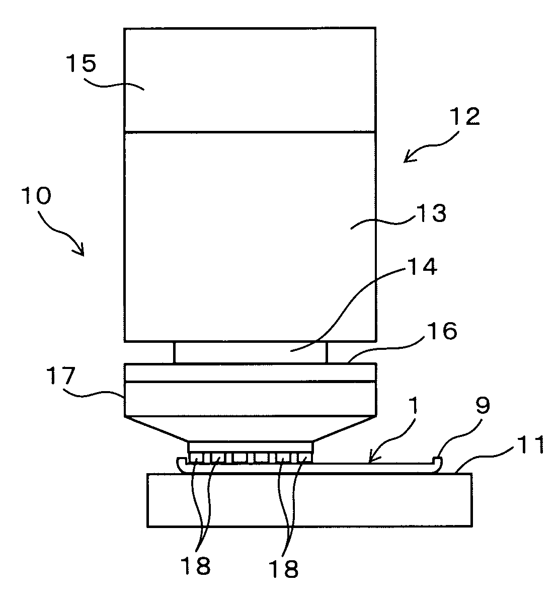
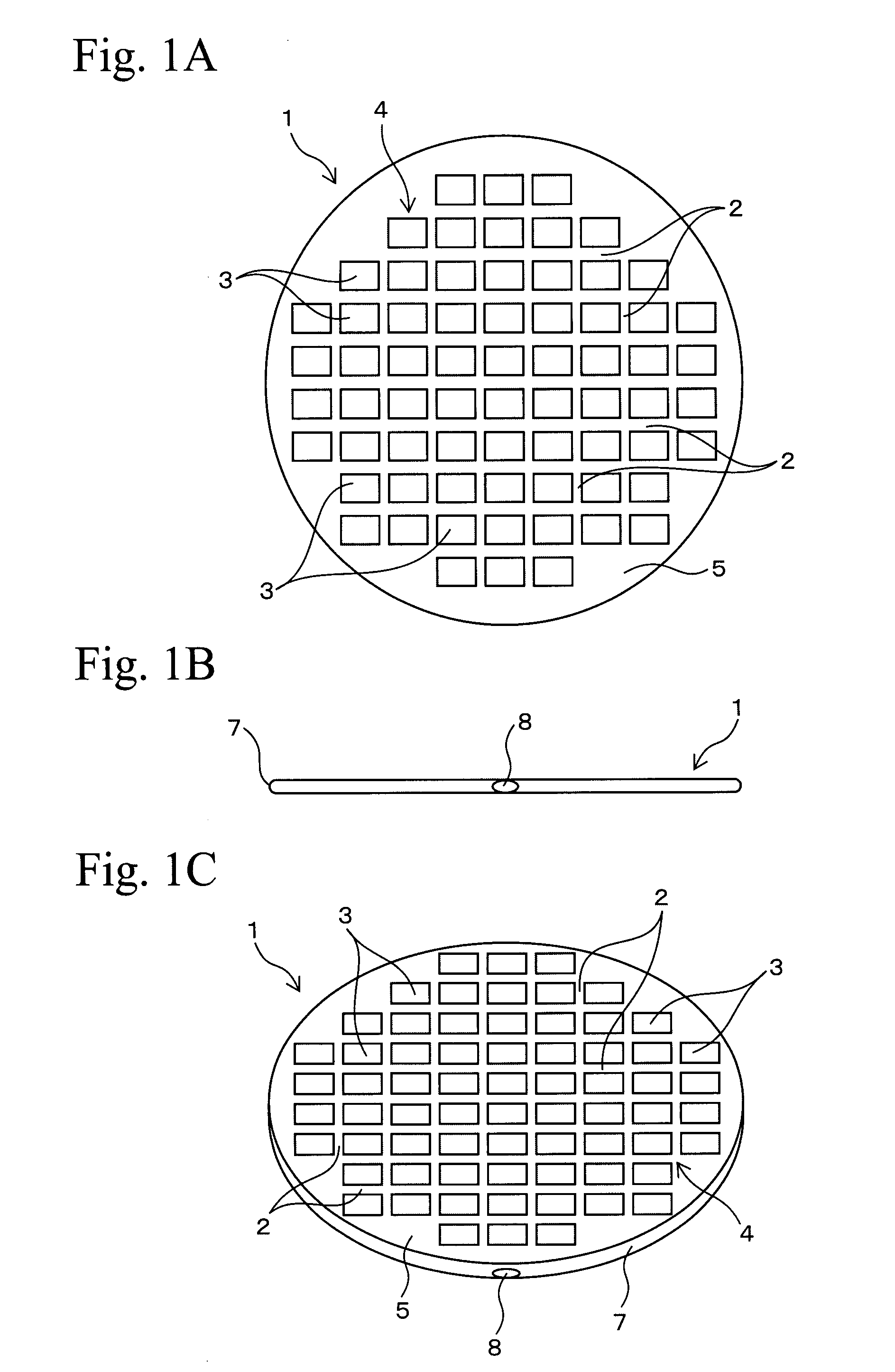
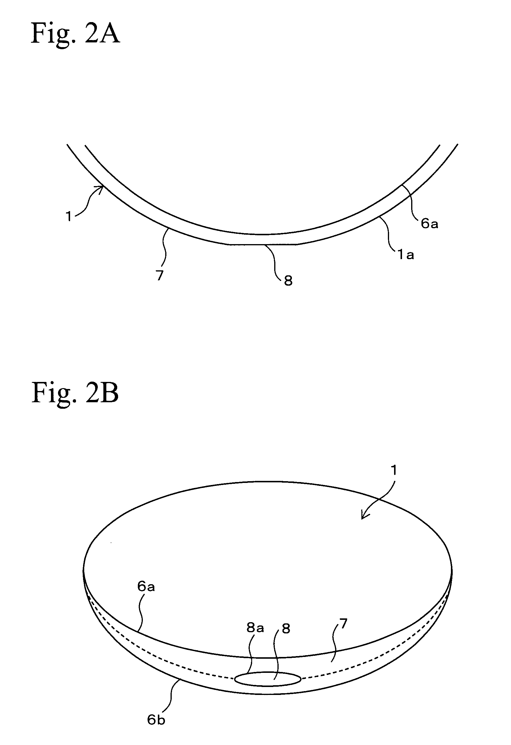
[0026]One embodiment according to the present invention will be explained hereinafter with reference to the drawings. FIGS. 1A to 1C show a semiconductor wafer (hereinafter referred to simply as a “wafer”) 1 which is composed of a single crystal silicon or the like and which is processed in one embodiment according to the present invention. For example, the wafer 1, which is disk-shaped and has a crystal orientation, has a thickness of about 600 μm. Grid-like predetermined division lines 2 are formed on a surface of the wafer 1, and plural rectangular semiconductor chips (devices) 3 are defined by the predetermined division lines 2 on the surface of the wafer 1. Electronic circuits are formed on surfaces of the semiconductor chips 3. The plural semiconductor chips 3 are formed on a device region 4 which is almost circular so as to be concentric with the wafer 1. A ring-shaped peripheral extra region 5 is formed around the device forming region 4.
[0027]As shown i...
PUM
 Abstract
Description
Claims
Application Information