Ridge-stripe semiconductor laser

a semiconductor laser and ridge-stripe technology, applied in semiconductor lasers, laser optical resonator construction, laser details, etc., can solve the problems of unstable laser light output, less effective stimulation emission, and reduced laser light output over time, so as to achieve the effect of reducing the optical confinement factor

Inactive Publication Date: 2009-07-21
PANASONIC CORP
View PDF5 Cites 21 Cited by
  • Summary
  • Abstract
  • Description
  • Claims
  • Application Information

AI Technical Summary

Benefits of technology

[0016]With the settings for the configuration of the laminated composite, the optical confinement factor can be made smaller on the forward side than on the backward side by, for example, structuring the insulating layer to include portions made of different materials and creating differences in refractive indexes a...

Problems solved by technology

As a result, the stimulated emission occurs less effectively although current is injected c...

Method used


Image

  • Ridge-stripe semiconductor laser
  • Ridge-stripe semiconductor laser
  • Ridge-stripe semiconductor laser

Examples


first embodiment

1. First Embodiment

[0029]1.1 Overall Configuration

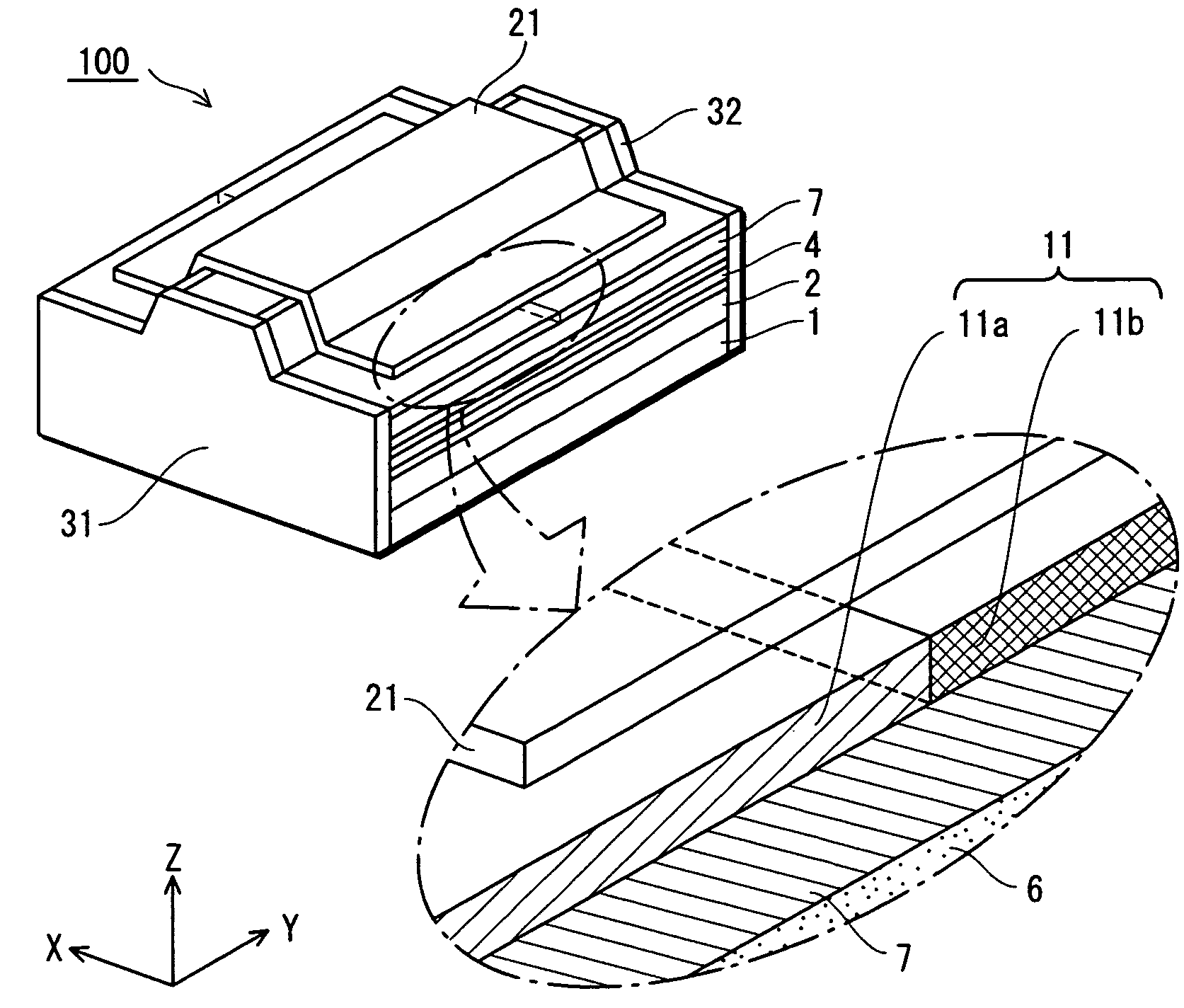
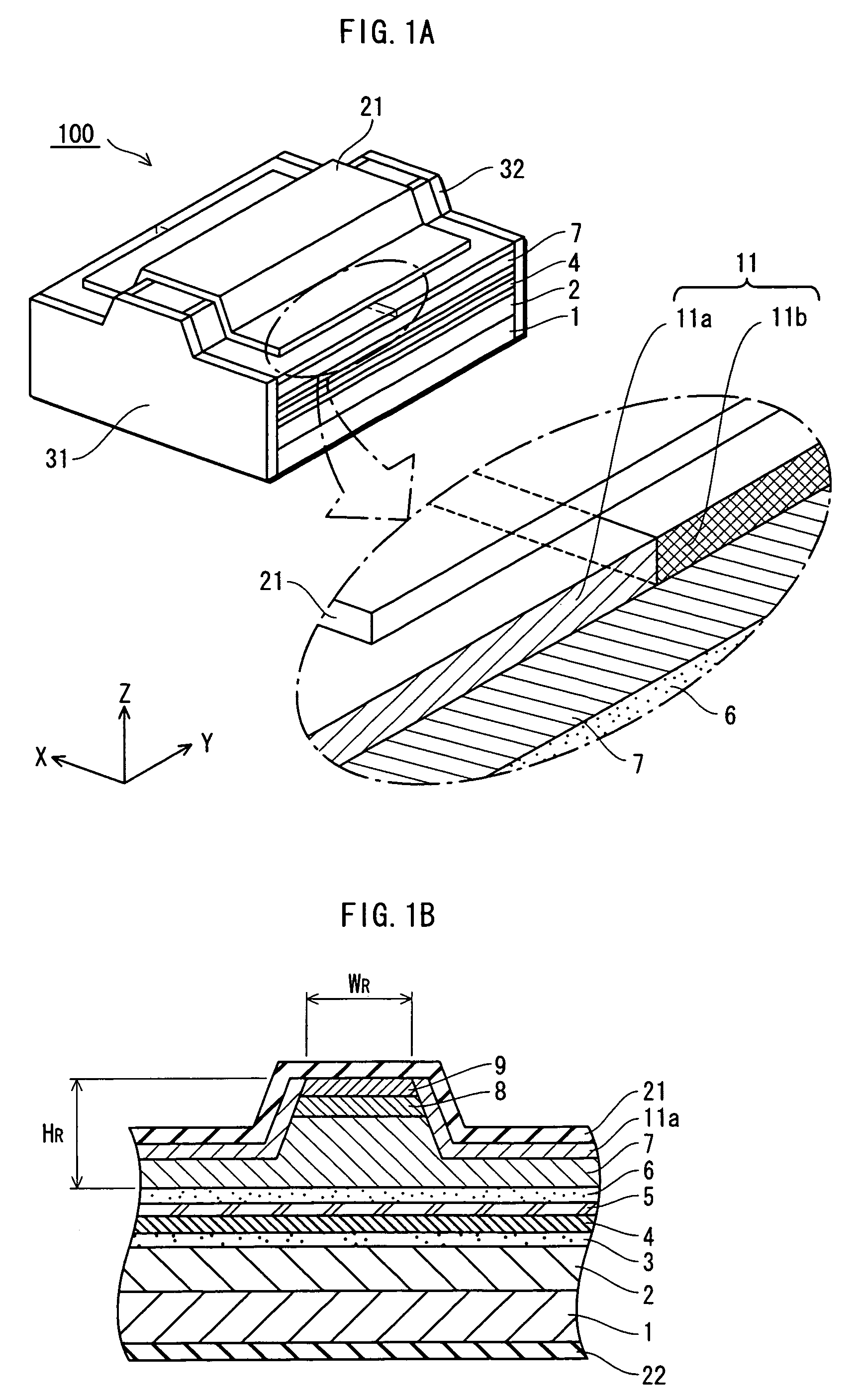
[0030]FIG. 1A is a perspective view of a semiconductor laser 100. The semiconductor laser 100 has the following configuration: a laminated composite is formed by including an n-type cladding layer 2 and a p-type cladding layer 7, between of which an active layer 4 is disposed, and a pair of dielectric multilayer films 31 and 32 are positioned at the end faces of the laminated composite.

[0031]FIG. 1B shows a schematic cross section of the semiconductor laser 100 and the above-mentioned laminated composite is composed of the following layers.

[0032]A substrate 1 is an n-type GaN substrate, having the dimensions of 300 μm in width, 600 μm in length, and 400 μm in thickness.

[0033]The n-type cladding layer 2 of n-type Al0.05Ga0.95N with a thickness of 1.2 μm is laid on the substrate 1. Disposed on the n-type cladding layer 2 is an n-type GaN optical guide layer 3 with a thickness of 0.05 μm.

[0034]The active layer 4 of InGaN with a thicknes...
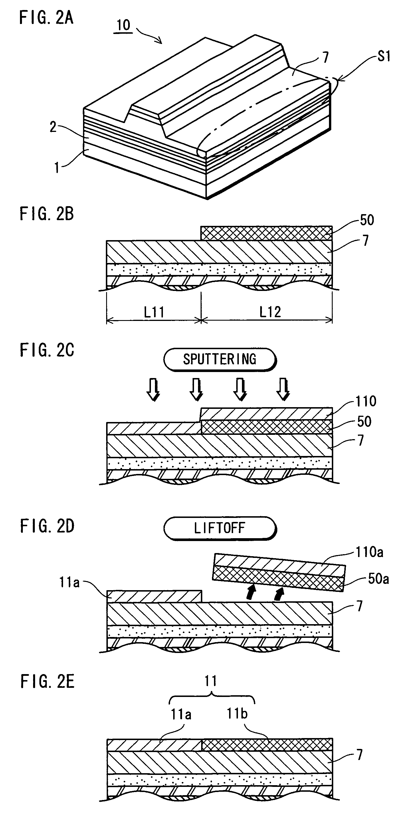
working example 1

The Semiconductor Laser 100 Where the Insulating Layer 11 of the Present Embodiment is Disposed

working example 2

The Semiconductor Laser 0.101 Where the Insulating Layer 12 of Modification 1 Above is Disposed


PUM


Abstract

A laminated composite includes: a 1st-conductive-type cladding layer laid on a substrate; an active layer laid on the 1st-conductive-type cladding layer; and a ridge-stripe 2nd-conductive-type cladding layer laid on the active layer. A pair of films is disposed at the end faces of the laminated composite so as to oppose each other along the lamination direction. The paired films are formed to have different spectral reflectances from each other. The resonator structure is formed with the laminated composite and the paired films. When, in the length direction of the resonator, a side with one of the paired films which has a smaller spectral reflectance is the forward side and a side with the other film having a larger spectral reflectance is the backward side, the laminated composite is structured so that the optical confinement factor becomes smaller on the forward side than on the backward side.

Description

BACKGROUND OF THE INVENTION[0001]1. Field of the Invention[0002]The present invention relates to a semiconductor laser used, for example, as a light source of an optical disc apparatus, in particular to a ridge-stripe semiconductor laser.[0003]2. Related Art[0004]Among semiconductor lasers, semiconductor lasers made of a III-V nitride semiconductor material (e.g. AlxGayIn1-x-y (provided that 0≦x≦1, 0≦y≦1)) are especially being developed to a practical level as a key device for a realization of super high density recording of optical disc apparatuses.[0005]Some semiconductor lasers have a configuration in which an n-type cladding layer 902, an active layer 904, and a p-type cladding layer 907 are formed in layers on a substrate 901, and a ridge is provided with the laminated composite, as shown in FIG. 9. A semiconductor laser 900 formed in this manner emits laser light outward according to the injected current (i.e. carriers) from a p-type electrode 921 covering the ridge and an n-t...

Claims


Application Information

Patent Timeline
IPC IPC(8): H01S5/00H01S5/10
CPCB82Y20/00H01S5/028H01S5/0287H01S5/34333H01S5/16H01S5/2214H01S5/0425H01S5/04252H01S2301/176
Inventor ITO, KEIJIKIDOGUCHI, ISAOYAJIMA, HIROYOSHI
Owner PANASONIC CORP
Why Eureka
Try Eureka